SLVSD44A September 2017 – July 2018 TPS63710
PRODUCTION DATA.
- 1 Features
- 2 Applications
- 3 Description
- 4 Revision History
- 5 Pin Configuration and Functions
- 6 Specifications
- 7 Detailed Description
- 8 Application and Implementation
- 9 Power Supply Recommendations
- 10Layout
- 11Device and Documentation Support
- 12Mechanical, Packaging, and Orderable Information
Package Options
Mechanical Data (Package|Pins)
- DRR|12
Thermal pad, mechanical data (Package|Pins)
- DRR|12
Orderable Information
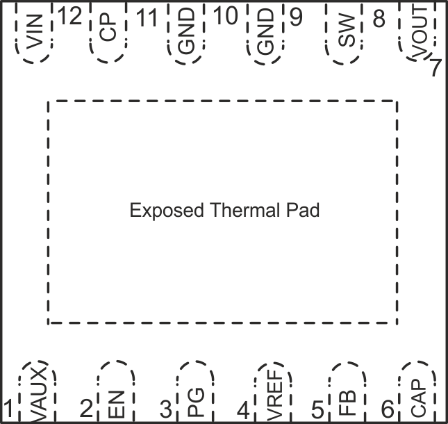
5 Pin Configuration and Functions
DRR Package
12-Pin WSON
Top View

Table 1. Pin Functions
| Pin | I/O | Description | |
|---|---|---|---|
| Name | No. | ||
| VIN | 12 | I | Power supply Input. Connect the input capacitor from this pin to GND and place it as close as possible to the device pins. |
| VAUX | 1 | O | Connect the output capacitor of the internal voltage regulator from this pin to GND. VAUX can be loaded externally with up to 100uA. Do not use this pin for any pulsed load to not couple noise into the internal supply. |
| GND | 10, 9 | Ground Connection. Voltages and signals are referenced to this pin. | |
| CP | 11 | O | Connect a capacitor from this pin to SW. |
| SW | 8 | O | Connect a capacitor from this pin to CP and the inductor from this pin to the output. |
| FB | 5 | I | Feedback pin for the voltage divider. |
| VOUT | 7 | I | Output voltage sense pin. |
| CAP | 6 | O | Reference system bypass capacitor connection. Do not tie anything other than a capacitor to GND to this pin. Keep any noise sources away from this pin. The capacitor connected to this pin forms a low-pass filter with an internal filter resistor and also defines the soft-start time. |
| VREF | 4 | O | Reference voltage output. Connect a voltage divider between this pin, FB and GND to set the output voltage. Do not connect any other circuitry to this pin. |
| EN | 2 | I | Enable pin. The device is enabled when the pin is connected to a logic high level e.g. VIN. The device is disabled when the pin is connected to a logic low level. The logic levels are referenced to the IC´s GND pin. |
| PG | 3 | O | Open drain power good output. Connect with a pull-up resistor to a positive voltage up to 5.5 V. If not used, leave open or connect to GND. |
| Exposed Thermal Pad | - | - | The thermal pad must be tied to GND. The pad must be soldered to a GND plane to achieve an appropriate thermal resistance and for mechanical reliability. |