SLVSD44A September   2017  – July 2018 TPS63710

PRODUCTION DATA.  

  1. Features
  2. Applications
  3. Description
    1.     Device Images
      1.      Typical Application
      2.      Efficiency vs output current for VOUT = -1.8V
  4. Revision History
  5. Pin Configuration and Functions
    1. Table 1. Pin Functions
  6. Specifications
    1. 6.1 Absolute Maximum Ratings
    2. 6.2 ESD Ratings
    3. 6.3 Recommended Operating Conditions
    4. 6.4 Thermal Information
    5. 6.5 Electrical Characteristics
    6. 6.6 Typical Characteristics
  7. Detailed Description
    1. 7.1 Overview
    2. 7.2 Functional Block Diagram
    3. 7.3 Feature Description
      1. 7.3.1 Low Noise Reference System
      2. 7.3.2 Duty Cycle
      3. 7.3.3 Enable
      4. 7.3.4 Undervoltage Lockout
      5. 7.3.5 Thermal Shutdown
      6. 7.3.6 Power Good Output
    4. 7.4 Device Functional Modes
      1. 7.4.1 Soft-Start
      2. 7.4.2 VOUT Discharge
      3. 7.4.3 Current Limit
      4. 7.4.4 CCP Capacitor Precharge
      5. 7.4.5 PWM Operation
  8. Application and Implementation
    1. 8.1 Application Information
    2. 8.2 Typical Application
      1. 8.2.1 Design Requirements
      2. 8.2.2 Detailed Design Procedure
        1. 8.2.2.1 Custom Design With WEBENCH® Tools
        2. 8.2.2.2 Setting the Output Voltage
        3. 8.2.2.3 Inductor Selection
        4. 8.2.2.4 Capacitor Selection
          1. 8.2.2.4.1 CCP Capacitor
          2. 8.2.2.4.2 Input Capacitor
          3. 8.2.2.4.3 Output Capacitor
      3. 8.2.3 Application Curves
        1. 8.2.3.1 Parameter Measurement Information
    3. 8.3 System Examples
      1. 8.3.1 Typical Application for Powering the Negative Rail of a Gallium Nitride (GaN) Power Amplifier
      2. 8.3.2 Typical Application for Powering the Negative Rail of an ADC or DAC
      3. 8.3.3 Typical Application for Laser Diode Bias
  9. Power Supply Recommendations
  10. 10Layout
    1. 10.1 Layout Guidelines
    2. 10.2 Layout Example
  11. 11Device and Documentation Support
    1. 11.1 Device Support
      1. 11.1.1 Custom Design With WEBENCH® Tools
      2. 11.1.2 Third-Party Products Disclaimer
    2. 11.2 Community Resources
    3. 11.3 Trademarks
    4. 11.4 Electrostatic Discharge Caution
    5. 11.5 Glossary
  12. 12Mechanical, Packaging, and Orderable Information

Package Options

Mechanical Data (Package|Pins)
Thermal pad, mechanical data (Package|Pins)
Orderable Information

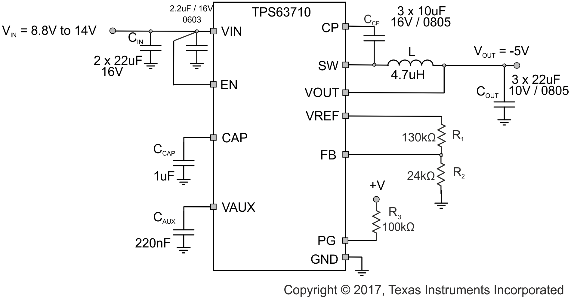
Typical Application for Powering the Negative Rail of a Gallium Nitride (GaN) Power Amplifier

The TPS63710 requires a supply voltage in the range of 8.8 V to 14 V in order to generate an output voltage of -5 V. The circuit therefore was optimized for this input voltage range. The number of the input, output and CCP capacitors have been adjusted to compensate for the higher dc bias effect with large input and output voltages. In addition, the inductor has been changed to 4.7 µH for low inductor current ripple at an input voltage up to 14 V.
TPS63710 TPS63710_5Vapplication.gifFigure 41. Typical Application for an Output Voltage of -5 V