SLVSEK4C July 2019 – February 2020 TPS63810 , TPS63811
PRODUCTION DATA.
- 1 Features
- 2 Applications
- 3 Description
- 4 Revision History
- 5 Device Comparison Table
- 6 Pin Configuration and Functions
- 7 Specifications
-
8 Detailed Description
- 8.1 Overview
- 8.2 Functional Block Diagram
- 8.3
Feature Description
- 8.3.1 Control Scheme
- 8.3.2 Control Scheme
- 8.3.3 Power-Save Mode Operation (PSM)
- 8.3.4 Forced-PWM Operation (FPWM)
- 8.3.5 Ramp-PWM Operation (RPWM)
- 8.3.6 Device Enable (EN)
- 8.3.7 Undervoltage Lockout (UVLO)
- 8.3.8 Soft Start
- 8.3.9 Output Voltage Control
- 8.3.10 Protection Functions
- 8.3.11 Power Good
- 8.3.12 Load Disconnect
- 8.3.13 Output Discharge
- 8.4 Device Functional Modes
- 8.5 Programming
- 8.6
Register Map
- 8.6.1
Register Description
- 8.6.1.1 Register Map
- 8.6.1.2 Register CONTROL (Slave address: 0b1110101; Register address: 0x01; Default: 0x00 or 0x20)
- 8.6.1.3 Register STATUS (Slave address: 0b1110101; Register address: 0x02; Default: 0x00)
- 8.6.1.4 Register DEVID (Slave address: 0b1110101; Register address: 0x03; Default: 0x04)
- 8.6.1.5 Register VOUT1 (Slave address: 0b1110101; Register address: 0x04; Default: 0x3C)
- 8.6.1.6 Register VOUT2 (Slave address: 0b1110101; Register address: 0x05; Default: 0x42)
- 8.6.1
Register Description
- 9 Application and Implementation
- 10Power Supply Recommendations
- 11Layout
- 12Device and Documentation Support
- 13Mechanical, Packaging, and Orderable Information
Package Options
Mechanical Data (Package|Pins)
- YFF|15
Thermal pad, mechanical data (Package|Pins)
Orderable Information
8.3.3 Power-Save Mode Operation (PSM)
To increase efficiency across a wide range of operating conditions, the device automatically changes from pulse-width modulation (PWM) at medium and high output currents to pulse-frequency modulation (PFM) at low output currents.
- During PWM operation, the device switches continuously and adjusts the duty cycle of each switching cycle to regulate the output voltage.
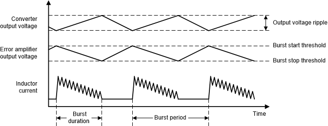
- During PFM operation, the device switches in bursts of a few switching cycles, separated by periods when the device does not switch (see Figure 13). PFM operation increases efficiency at low output currents because when the device does not switch, there are no switching losses and most of the internal circuitry is disabled, which reduces quiescent power consumption. A comparator with hysteresis compares the output voltage of the error amplifier to a predefined PFM threshold voltage. When the output voltage of the error amplifier is greater than the burst threshold voltage, the device starts switching. When the output voltage of the error amplifier is less than the burst threshold voltage, the device stops switching. This scheme automatically adjusts the frequency and the duration of the switching bursts to regulate the output voltage. During PFM operation, the output voltage ripple can be higher and the transient response is not as good as during PWM operation (see Table 1).
To enable power-save mode, clear the FPWM bit in the Control register to 0.
 Figure 13. Pulse-Frequency Modulation
 WHITESPACE
Table 1. Forced-PWM versus Power-Save Mode Performance Comparison
| PERFORMANCE PARAMETER | BEST OPERATING MODE |
|---|---|
| Low-power efficiency | Power-Save Mode (PSM) |
| Medium- and high-power efficiency | No difference |
| DC Output voltage accuracy | Forced-PWM |
| Transient response | Forced-PWM |
| Output voltage ripple | Forced-PWM |
WHITESPACE