SLVSET3D March   2020  – October 2020 TPS63900

PRODUCTION DATA  

  1. Features
  2. Applications
  3. Description
  4. Revision History
  5. Pin Configuration and Functions
  6. Specifications
    1. 6.1 Absolute Maximum Ratings
    2. 6.2 ESD Ratings
    3. 6.3 Recommended Operating Conditions
    4. 6.4 Thermal Information
    5. 6.5 Electrical Characteristics
    6. 6.6 Typical Characteristics
  7. Detailed Description
    1. 7.1 Overview
    2. 7.2 Functional Block Diagram
    3. 7.3 Feature Description
      1. 7.3.1 Trapezoidal Current Control
      2. 7.3.2 Device Enable / Disable
      3. 7.3.3 Soft Start
      4. 7.3.4 Input Current Limit
      5. 7.3.5 Dynamic Voltage Scaling
      6. 7.3.6 Device Configuration (Resistor-to-Digital Interface)
      7. 7.3.7 SEL Pin
      8. 7.3.8 Short-Circuit Protection
        1. 7.3.8.1 Current Limit Setting = 'Unlimited'
        2. 7.3.8.2 Current Limit Setting = 1 mA to 100 mA
      9. 7.3.9 Thermal Shutdown
    4. 7.4 Device Functional Modes
  8. Application and Implementation
    1. 8.1 Application Information
    2. 8.2 Typical Application
      1. 8.2.1 Design Requirements
      2. 8.2.2 Detailed Design Procedure
        1. 8.2.2.1 Custom Design with WEBENCH Tools
        2. 8.2.2.2 Inductor Selection
        3. 8.2.2.3 Output Capacitor Selection
        4. 8.2.2.4 Input Capacitor Selection
        5. 8.2.2.5 Setting The Output Voltage
      3. 8.2.3 Application Curves
  9. Power Supply Recommendations
  10. 10Layout
    1. 10.1 Layout Guidelines
    2. 10.2 Layout Example
  11. 11Device and Documentation Support
    1. 11.1 Device Support
      1. 11.1.1 Third-Party Products Disclaimer
    2. 11.2 Documentation Support
      1. 11.2.1 Related Documentation
    3. 11.3 Receiving Notification of Documentation Updates
    4. 11.4 Support Resources
    5. 11.5 Trademarks
    6. 11.6 Electrostatic Discharge Caution
    7. 11.7 Glossary
  12. 12Mechanical, Packaging, and Orderable Information

Package Options

Mechanical Data (Package|Pins)
Thermal pad, mechanical data (Package|Pins)
Orderable Information

Dynamic Voltage Scaling

The device has a dynamic voltage scaling function to switch between the two output voltage settings. When the SEL pin changes state, the output voltage ramps to the new value in 100-mV steps. The duration of each step is 125 µs (see Figure 7-10).

The device does not actively discharge the output capacitor, when the output voltage ramps to a lower level. This leads to a longer output voltage settling time when light load is applied (see Figure 7-11). The settling time can be calculated with Equation 3.

Equation 3. GUID-49EF34BB-5589-4E14-9A19-4E2537401444-low.gif
GUID-F486D684-9BEA-42DA-B16F-CC56FE6B5CF2-low.gif
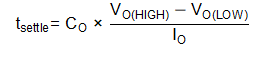
Figure 7-10 Dynamic Voltage Scaling with High Load
GUID-2539F7DD-CC11-492C-9D46-73EB3A2DDFBD-low.gifFigure 7-11 Dynamic Voltage Scaling with Light Load