SLVS551A December 2004 – September 2015 TPS65014
PRODUCTION DATA.
- 1 Features
- 2 Applications
- 3 Description
- 4 Revision History
- 5 Pin Configuration and Functions
-
6 Specifications
- 6.1 Absolute Maximum Ratings
- 6.2 ESD Ratings
- 6.3 Recommended Operating Conditions
- 6.4 Thermal Information
- 6.5 Electrical Characteristics
- 6.6 Electrical Characteristics: Battery Charger
- 6.7 Dissipation Ratings
- 6.8 Serial Interface Timing Requirements
- 6.9 Switching Characteristics
- 6.10 Typical Characteristics
-
7 Detailed Description
- 7.1 Overview
- 7.2 Functional Block Diagram
- 7.3 Feature Description
- 7.4 Device Functional Modes
- 7.5
Register Maps
- 7.5.1 CHGSTATUS Register (offset = 01h) (reset: 00h)
- 7.5.2 REGSTATUS Register (offset = 02h) (reset: 00h)
- 7.5.3 MASK1 Register (offset = 03h) (reset: FFh)
- 7.5.4 MASK2 Register (offset = 04h) (reset: FFh)
- 7.5.5 ACKINT1 Register (offset = 05h) (reset: 00h)
- 7.5.6 ACKINT2 Register (offset: 06h) (reset: 00h)
- 7.5.7 CHGCONFIG Register (offset: 07h) (reset: 1Bh)
- 7.5.8 LED1_ON Register (offset: 08h) (reset: 00h)
- 7.5.9 LED1_PER Register (offset: 09h) (reset: 00h)
- 7.5.10 LED2_ON Register (offset: 0Ah) (reset: 00h)
- 7.5.11 LED2_PER (offset: 0Bh) (reset: 00h)
- 7.5.12 VDCDC1 Register (offset: 0Ch) (reset: 32h/33h)
- 7.5.13 VDCDC2 Register (offset: 0Dh) (reset: 60h/70h)
- 7.5.14 VREGS1 Register (offset: 0Eh) (reset: 88h)
- 7.5.15 MASK3 Register (offset: 0Fh) (reset: 00h)
- 7.5.16 DEFGPIO Register (offset = 10h) (reset: 00h)
- 8 Application and Implementation
- 9 Power Supply Recommendations
- 10Layout
- 11Device and Documentation Support
- 12Mechanical, Packaging, and Orderable Information
Package Options
Mechanical Data (Package|Pins)
- RGZ|48
Thermal pad, mechanical data (Package|Pins)
- RGZ|48
Orderable Information
1 Features
- Linear Charger Management for Single Li-Ion or Li-Polymer Cells
- Dual Input Ports for Charging From USB or From Wall Plug, Handles 100-mA and 500-mA USB Requirements
- Charge Current Programmable Through External Resistor
- 1-A, 95% Efficient Step-Down Converter for I/O and Peripheral Components (VMAIN)
- 400-mA, 90% Efficient Step-Down Converter for Processor Core (VCORE)
- 2× 200-mA LDOs for I/O and Peripheral Components, LDO Enable Through Bus
- Serial Interface Compatible With I2C, Supports 100-kHz, 400-kHz Operation
- LOW_PWR Pin to Lower or Disable Processor Core Supply Voltage in Deep-Sleep Mode
- 70-µA Quiescent Current
- 1% Reference Voltage
- Thermal-Shutdown Protection
2 Applications
- All Single Li-Ion Cell-Operated Products Requiring Multiple Supplies Including:
- PDAs
- Cellular and Smart Phones
- Internet Audio Players
- Digital Still Cameras
- Digital Radio Players
- Split-Supply DSP and µP Solutions
3 Description
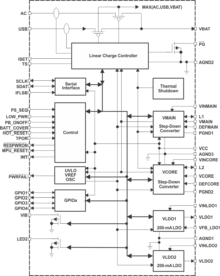
The TPS65014 device is an integrated power- and battery-management IC for applications powered by one Li-ion or Li-polymer cell and which require multiple power rails. The TPS65014 provides two highly efficient, step-down converters targeted at providing the core voltage and peripheral I/O rails in a processor-based system. Both step-down converters enter a low-power mode at light load for maximum efficiency across the widest possible range of load currents. The LOW_PWR pin allows the core converter to lower its output voltage when the application processor goes into deep sleep. The TPS65014 also integrates two 200-mA LDO voltage regulators, which are enabled through the serial interface. Each LDO operates with an input voltage range of 1.8 V to 6.5 V, thus allowing them to be supplied from one of the step-down converters or directly from the battery.
Device Information(1)
| PART NUMBER | PACKAGE | BODY SIZE (NOM) |
|---|---|---|
| TPS65014 | VQFN (48) | 7.00 mm × 7.00 mm |
- For all available packages, see the orderable addendum at the end of the data sheet.
Functional Block Diagram
