SLVS950I July   2009  – May 2018 TPS65070 , TPS65072 , TPS65073 , TPS650731 , TPS650732

UNLESS OTHERWISE NOTED, this document contains PRODUCTION DATA.  

  1. Features
  2. Applications
  3. Description
    1.     Block Diagram
  4. Revision History
  5. Description (continued)
  6. Device Options
  7. Pin Configuration and Functions
    1.     Pin Functions
  8. Specifications
    1. 8.1  Absolute Maximum Ratings
    2. 8.2  ESD Ratings
    3. 8.3  Recommended Operating Conditions
    4. 8.4  Thermal Information
    5. 8.5  Electrical Characteristics
    6. 8.6  Electrical Characteristics - DCDC1 Converter
    7. 8.7  Electrical Characteristics - DCDC2 Converter
    8. 8.8  Electrical Characteristics - DCDC3 Converter
    9. 8.9  Electrical Characteristics - VLDO1 and VLDO2 Low Dropout Regulators
    10. 8.10 Electrical Characteristics - wLED Boost Converter
    11. 8.11 Electrical Characteristics - Reset, PB_IN, PB_OUT, PGood, Power_on, INT, EN_EXTLDO, EN_wLED
    12. 8.12 Electrical Characteristics - ADC Converter
    13. 8.13 Electrical Characteristics - Touch Screen Interface
    14. 8.14 Electrical Characteristics - Power Path
    15. 8.15 Electrical Characteristics - Battery Charger
    16. 8.16 Timing Requirements
    17. 8.17 Dissipation Ratings
    18. 8.18 Typical Characteristics
  9. Parameter Measurement Information
  10. 10Detailed Description
    1. 10.1 Overview
    2. 10.2 Functional Block Diagram
    3. 10.3 Feature Description
      1. 10.3.1  Battery Charger and Power Path
      2. 10.3.2  Power Down
      3. 10.3.3  Power-On Reset
      4. 10.3.4  Power-Path Management
        1. 10.3.4.1 SYS Output
      5. 10.3.5  Battery Charging
        1. 10.3.5.1 I-PRECHARGE
        2. 10.3.5.2 ITERM
        3. 10.3.5.3 Battery Detection and Recharge
        4. 10.3.5.4 Charge Termination On/Off
        5. 10.3.5.5 Timers
        6. 10.3.5.6 Dynamic Timer Function
        7. 10.3.5.7 Timer Fault
      6. 10.3.6  Battery Pack Temperature Monitoring
      7. 10.3.7  Battery Charger State Diagram
      8. 10.3.8  DC-DC Converters and LDOs
        1. 10.3.8.1 Operation
        2. 10.3.8.2 DCDC1 Converter
        3. 10.3.8.3 DCDC2 Converter
        4. 10.3.8.4 DCDC3 Converter
      9. 10.3.9  Power Save Mode
        1. 10.3.9.1 Dynamic Voltage Positioning
        2. 10.3.9.2 100% Duty Cycle Low Dropout Operation
        3. 10.3.9.3 Undervoltage Lockout
      10. 10.3.10 Short-Circuit Protection
        1. 10.3.10.1 Soft Start
      11. 10.3.11 Enable
        1. 10.3.11.1 RESET (TPS65070, TPS65073, TPS650731, TPS650732 Only)
        2. 10.3.11.2 PGOOD (Reset Signal For Applications Processor)
        3. 10.3.11.3 PB_IN (Push-Button IN)
        4. 10.3.11.4 PB_OUT
        5. 10.3.11.5 POWER_ON
        6. 10.3.11.6 EN_wLED (TPS65072 Only)
        7. 10.3.11.7 EN_EXTLDO (TPS65072 Only)
      12. 10.3.12 Short-Circuit Protection
      13. 10.3.13 Thermal Shutdown
        1. 10.3.13.1 Low Dropout Voltage Regulators
        2. 10.3.13.2 White LED Boost Converter
        3. 10.3.13.3 A/D Converter
        4. 10.3.13.4 Touch Screen Interface (only for TPS65070, TPS65073, TPS650731, TPS650732)
          1. 10.3.13.4.1 Performing Measurements Using the Touch Screen Controller
    4. 10.4 Device Functional Modes
    5. 10.5 Programming
      1. 10.5.1 I2C Interface Specification
        1. 10.5.1.1 Serial interface
    6. 10.6 Register Maps
      1. 10.6.1  PPATH1. Register Address: 01h
      2. 10.6.2  INT. Register Address: 02h
      3. 10.6.3  CHGCONFIG0. Register Address: 03h
      4. 10.6.4  CHGCONFIG1. Register Address: 04h
      5. 10.6.5  CHGCONFIG2. Register Address: 05h
      6. 10.6.6  CHGCONFIG3. Register Address: 06h
      7. 10.6.7  ADCONFIG. Register Address: 07h
      8. 10.6.8  TSCMODE. Register Address: 08h
      9. 10.6.9  ADRESULT_1. Register Address: 09h
      10. 10.6.10 ADRESULT_2. Register Address: 0Ah
      11. 10.6.11 PGOOD. Register Address: 0Bh
      12. 10.6.12 PGOODMASK. Register Address: 0Ch
      13. 10.6.13 CON_CTRL1. Register Address: 0Dh
      14. 10.6.14 CON_CTRL2. Register Address: 0Eh
      15. 10.6.15 CON_CTRL3. Register Address: 0Fh
      16. 10.6.16 DEFDCDC1. Register Address: 10h
      17. 10.6.17 DEFDCDC2_LOW. Register Address: 11h
      18. 10.6.18 DEFDCDC2_HIGH. Register Address: 12h
      19. 10.6.19 DEFDCDC3_LOW. Register Address: 13h
      20. 10.6.20 DEFDCDC3_HIGH. Register Address: 14h
      21. 10.6.21 DEFSLEW. Register Address: 15h
      22. 10.6.22 LDO_CTRL1. Register Address: 16h
      23. 10.6.23 DEFLDO2. Register Address: 17h
      24. 10.6.24 WLED_CTRL1. Register Address: 18h
      25. 10.6.25 WLED_CTRL2. Register Address: 19h
  11. 11Application and Implementation
    1. 11.1 Application Information
      1. 11.1.1 Power Solutions For Different Application Processors
        1. 11.1.1.1 Default Settings
        2. 11.1.1.2 Starting TPS6507x
    2. 11.2 Typical Applications
      1. 11.2.1 General PMIC Application
        1. 11.2.1.1 Design Requirements
        2. 11.2.1.2 Detailed Design Procedure
          1. 11.2.1.2.1 Output Filter Design (Inductor and Output Capacitor)
            1. 11.2.1.2.1.1 Inductor Selection
            2. 11.2.1.2.1.2 Output Capacitor Selection
            3. 11.2.1.2.1.3 Input Capacitor Selection/Input Voltage
            4. 11.2.1.2.1.4 Output Voltage Selection
            5. 11.2.1.2.1.5 Voltage Change on DCDC2 and DCDC3
          2. 11.2.1.2.2 LDOs
            1. 11.2.1.2.2.1 Output Capacitor Selection
            2. 11.2.1.2.2.2 Input Capacitor Selection
            3. 11.2.1.2.2.3 Output Voltage Change For LDO1 and LDO2
            4. 11.2.1.2.2.4 Unused LDOs
          3. 11.2.1.2.3 White-LED Boost Converter
            1. 11.2.1.2.3.1 LED-Current Setting/Dimming
            2. 11.2.1.2.3.2 Setup
            3. 11.2.1.2.3.3 Setting the LED Current
            4. 11.2.1.2.3.4 Inductor Selection
            5. 11.2.1.2.3.5 Diode Selection
            6. 11.2.1.2.3.6 Output Capacitor Selection
            7. 11.2.1.2.3.7 Input Capacitor Selection
          4. 11.2.1.2.4 Battery Charger
            1. 11.2.1.2.4.1 Temperature Sensing
            2. 11.2.1.2.4.2 Changing the Charging Temperature Range (Default 0°C to 45°C)
        3. 11.2.1.3 Application Curves
      2. 11.2.2 Powering OMAP-L138
        1. 11.2.2.1 Design Requirements
        2. 11.2.2.2 Detailed Design Procedure
      3. 11.2.3 Powering Atlas IV
        1. 11.2.3.1 Design Requirements
        2. 11.2.3.2 Detailed Design Procedure
          1. 11.2.3.2.1 Prima SLEEP Mode and DEEP SLEEP Mode Support
          2. 11.2.3.2.2 SLEEP Mode
          3. 11.2.3.2.3 DEEP SLEEP Mode
      4. 11.2.4 OMAP35xx (Supporting SYS-OFF Mode)
        1. 11.2.4.1 Design Requirements
        2. 11.2.4.2 Detailed Design Procedure
      5. 11.2.5 TPS650731 for OMAP35xx
        1. 11.2.5.1 Design Requirements
        2. 11.2.5.2 Detailed Design Procedure
      6. 11.2.6 Powering AM3505 Using TPS650732
        1. 11.2.6.1 Design Requirements
        2. 11.2.6.2 Detailed Design Procedure
  12. 12Power Supply Recommendations
  13. 13Layout
    1. 13.1 Layout Guidelines
    2. 13.2 Layout Example
  14. 14Device and Documentation Support
    1. 14.1 Device Support
      1. 14.1.1 Third-Party Products Disclaimer
    2. 14.2 Documentation Support
      1. 14.2.1 Related Documentation
    3. 14.3 Related Links
    4. 14.4 Receiving Notification of Documentation Updates
    5. 14.5 Community Resources
    6. 14.6 Trademarks
    7. 14.7 Electrostatic Discharge Caution
    8. 14.8 Glossary
  15. 15Mechanical, Packaging, and Orderable Information

Package Options

Mechanical Data (Package|Pins)
Thermal pad, mechanical data (Package|Pins)
Orderable Information

Battery Charger and Power Path

The TPS6507x integrates a Li-ion linear charger and system power path management targeted at space-limited portable applications. The TPS6507x power the system while simultaneously and independently charging the battery. This feature reduces the number of charge and discharge cycles on the battery, allows for proper charge termination and enables the system to run with a defective or absent battery pack. It also allows instant system turn-on even with a totally discharged battery. The input power source for charging the battery and running the system can be an AC adapter or an USB port. The power-path management feature automatically reduces the charging current if the system load increases. The power-path architecture also permits the battery to supplement the system current requirements when the adapter cannot deliver the peak system currents.
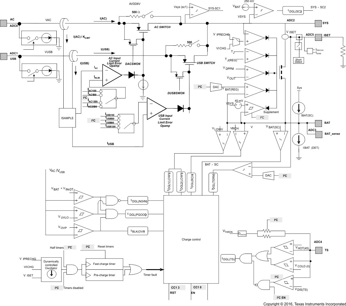
TPS65070 TPS65072 TPS65073 TPS650731 TPS650732 chg_bd_lvs950.gifFigure 26. Charger Block Diagram