SLVS493E March   2004  – April 2022 TPS65130 , TPS65131

PRODUCTION DATA  

  1. Features
  2. Applications
  3. Description
  4. Revision History
  5. Pin Configuration and Functions
  6. Specifications
    1. 6.1 Absolute Maximum Ratings
    2. 6.2 ESD Ratings
    3. 6.3 Recommended Operating Conditions
    4. 6.4 Thermal Information
    5. 6.5 Electrical Characteristics
    6. 6.6 Switching Characteristics
    7. 6.7 Typical Characteristics
  7. Detailed Description
    1. 7.1 Overview
    2. 7.2 Functional Block Diagram
    3. 7.3 Feature Description
      1. 7.3.1 Power Conversion
      2. 7.3.2 Control
      3. 7.3.3 Enable
      4. 7.3.4 Load Disconnect
      5. 7.3.5 Soft-Start
      6. 7.3.6 Overvoltage Protection
      7. 7.3.7 Undervoltage Lockout
      8. 7.3.8 Overtemperature Shutdown
    4. 7.4 Device Functional Modes
      1. 7.4.1 Power-Save Mode
      2. 7.4.2 Full Operation with VIN > 2.7 V
      3. 7.4.3 Limited Operation with VUVLO < VIN < 2.7 V
      4. 7.4.4 No Operation with VIN < VUVLO
  8. Applications and Implementation
    1. 8.1 Application Information
    2. 8.2 Typical Application
      1. 8.2.1 Design Requirements
      2. 8.2.2 Detailed Design Procedure
        1. 8.2.2.1 Programming the Output Voltage
          1. 8.2.2.1.1 Boost Converter
          2. 8.2.2.1.2 Inverting Converter
        2. 8.2.2.2 Inductor Selection
        3. 8.2.2.3 Capacitor Selection
          1. 8.2.2.3.1 Input Capacitor
          2. 8.2.2.3.2 Output Capacitors
        4. 8.2.2.4 Rectifier Diode Selection
        5. 8.2.2.5 External PMOS Selection
        6. 8.2.2.6 Stabilizing the Control Loop
          1. 8.2.2.6.1 Feedforward Capacitor
          2. 8.2.2.6.2 Compensation Capacitors
      3. 8.2.3 Analog Supply Filter
        1. 8.2.3.1 RC-Filter
        2. 8.2.3.2 LC-Filter
      4. 8.2.4 Application Curves
  9. Layout
    1. 9.1 Layout Guidelines
    2. 9.2 Layout Example
    3. 9.3 Thermal Considerations
  10. 10Device and Documentation Support
    1. 10.1 Device Support
    2. 10.2 Receiving Notification of Documentation Updates
    3. 10.3 Support Resources
    4. 10.4 Trademarks
    5. 10.5 Electrostatic Discharge Caution
    6. 10.6 Glossary
  11. 11Mechanical, Packaging, and Orderable Information

Package Options

Refer to the PDF data sheet for device specific package drawings

Mechanical Data (Package|Pins)
  • RGE|24
Thermal pad, mechanical data (Package|Pins)
Orderable Information
Inverting Converter

The output voltage of the inverting converter stage can also be adjusted with an external resistor divider. It must be connected to the FBN pin. Unlike the feedback divider at the boost converter, the reference point of the feedback divider is not GND but VREF. So the typical value of the voltage at the FBN pin is 0 V. The minimum recommended output voltage at the inverting converter is –15 V. Feedback divider current considerations are similar to the considerations at the boost converter. For the same reasons, the feedback divider current should be in the range of 5 µA or greater. The voltage across R4 is 1.213 V. Based on those values, the recommended value for R4 should be lower than 200 kΩ to set the divider current at the required value.

Calculate the value of resistor R3, as a function of the needed output voltage (VNEG), with Equation 2:

Equation 2. GUID-B2E6A4D0-73ED-410D-ADB0-277D6E56B755-low.gif

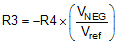
In this example, with R4 = 121.2 kΩ, choose R3 = 1 MΩ to set VNEG = –10 V.