SLVS493E March 2004 – April 2022 TPS65130 , TPS65131
PRODUCTION DATA
- 1 Features
- 2 Applications
- 3 Description
- 4 Revision History
- 5 Pin Configuration and Functions
- 6 Specifications
- 7 Detailed Description
-
8 Applications and Implementation
- 8.1 Application Information
- 8.2
Typical Application
- 8.2.1 Design Requirements
- 8.2.2 Detailed Design Procedure
- 8.2.3 Analog Supply Filter
- 8.2.4 Application Curves
- 9 Layout
- 10Device and Documentation Support
- 11Mechanical, Packaging, and Orderable Information
Package Options
Refer to the PDF data sheet for device specific package drawings
Mechanical Data (Package|Pins)
- RGE|24
Thermal pad, mechanical data (Package|Pins)
- RGE|24
Orderable Information
6.7 Typical Characteristics
At 25°C, unless otherwise noted.
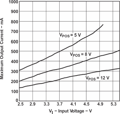 Figure 6-1 TPS65130 Maximum Output Current (VPOS) vs Input Voltage
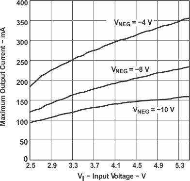 Figure 6-3 TPS65130 Maximum Output Current (VNEG) vs Input Voltage
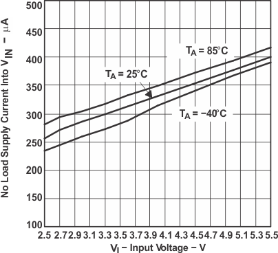 Figure 6-5 No Load Supply Current into VIN vs Input Voltage
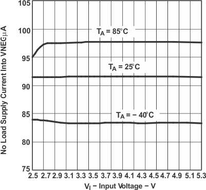 Figure 6-7 No Load Supply Current into VNEG vs Input Voltage
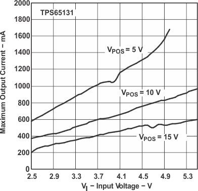 Figure 6-2 TPS65131 Maximum Output Current (VPOS) vs input Voltage
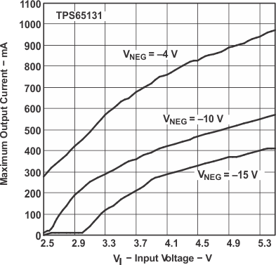 Figure 6-4 TPS65131 Maximum Output Current (VNEG) vs Input Voltage
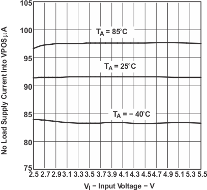 Figure 6-6 No Load Supply Current into VPOS vs Input Voltage