SLDS187A October 2018 – December 2019 TPS65216
PRODUCTION DATA.
- 1 Device Overview
- 2 Revision History
- 3 Pin Configuration and Functions
- 4 Specifications
-
5 Detailed Description
- 5.1 Overview
- 5.2 Functional Block Diagram
- 5.3
Feature Description
- 5.3.1
Wake-Up and Power-Up and Power-Down Sequencing
- 5.3.1.1 Power-Up Sequencing
- 5.3.1.2 Power-Down Sequencing
- 5.3.1.3 Strobe 1 and Strobe 2
- 5.3.1.4 Supply Voltage Supervisor and Power-Good (PGOOD)
- 5.3.1.5 Internal LDO (INT_LDO)
- 5.3.1.6 Current Limited Load Switch
- 5.3.1.7 LDO1
- 5.3.1.8 UVLO
- 5.3.1.9 Power-Fail Comparator
- 5.3.1.10 DCDC3 and DCDC4 Power-Up Default Selection
- 5.3.1.11 I/O Configuration
- 5.3.1.12 Push Button Input (PB)
- 5.3.1.13 AC_DET Input (AC_DET)
- 5.3.1.14 Interrupt Pin (INT)
- 5.3.1.15 I2C Bus Operation
- 5.3.1
Wake-Up and Power-Up and Power-Down Sequencing
- 5.4 Device Functional Modes
- 5.5
Register Maps
- 5.5.1 Password Protection
- 5.5.2 FLAG Register
- 5.5.3
TPS65216 Registers
- 5.5.3.1 CHIPID Register (subaddress = 0x00) [reset = 0x05]
- 5.5.3.2 INT1 Register (subaddress = 0x01) [reset = 0x00]
- 5.5.3.3 INT2 Register (subaddress = 0x02) [reset = 0x00]
- 5.5.3.4 INT_MASK1 Register (subaddress = 0x03) [reset = 0x00]
- 5.5.3.5 INT_MASK2 Register (subaddress = 0x04) [reset = 0x00]
- 5.5.3.6 STATUS Register (subaddress = 0x05) [reset = 00XXXXXXb]
- 5.5.3.7 CONTROL Register (subaddress = 0x06) [reset = 0x00]
- 5.5.3.8 FLAG Register (subaddress = 0x07) [reset = 0x00]
- 5.5.3.9 PASSWORD Register (subaddress = 0x10) [reset = 0x00]
- 5.5.3.10 ENABLE1 Register (subaddress = 0x11) [reset = 0x00]
- 5.5.3.11 ENABLE2 Register (subaddress = 0x12) [reset = 0x00]
- 5.5.3.12 CONFIG1 Register (subaddress = 0x13) [reset = 0x4C]
- 5.5.3.13 CONFIG2 Register (subaddress = 0x14) [reset = 0xC0]
- 5.5.3.14 CONFIG3 Register (subaddress = 0x15) [reset = 0x0]
- 5.5.3.15 DCDC1 Register (offset = 0x16) [reset = 0x99]
- 5.5.3.16 DCDC2 Register (subaddress = 0x17) [reset = 0x99]
- 5.5.3.17 DCDC3 Register (subaddress = 0x18) [reset = 0x8C]
- 5.5.3.18 DCDC4 Register (subaddress = 0x19) [reset = 0xB2]
- 5.5.3.19 SLEW Register (subaddress = 0x1A) [reset = 0x06]
- 5.5.3.20 LDO1 Register (subaddress = 0x1B) [reset = 0x1F]
- 5.5.3.21 SEQ1 Register (subaddress = 0x20) [reset = 0x00]
- 5.5.3.22 SEQ2 Register (subaddress = 0x21) [reset = 0x00]
- 5.5.3.23 SEQ3 Register (subaddress = 0x22) [reset = 0x98]
- 5.5.3.24 SEQ4 Register (subaddress = 0x23) [reset = 0x75]
- 5.5.3.25 SEQ5 Register (subaddress = 0x24) [reset = 0x12]
- 5.5.3.26 SEQ6 Register (subaddress = 0x25) [reset = 0x63]
- 5.5.3.27 SEQ7 Register (subaddress = 0x26) [reset = 0x03]
- 6 Application and Implementation
- 7 Power Supply Recommendations
- 8 Layout
- 9 Device and Documentation Support
- 10Mechanical, Packaging, and Orderable Information
Package Options
Mechanical Data (Package|Pins)
- RSL|48
Thermal pad, mechanical data (Package|Pins)
- RSL|48
Orderable Information
5.3.1.5 Internal LDO (INT_LDO)
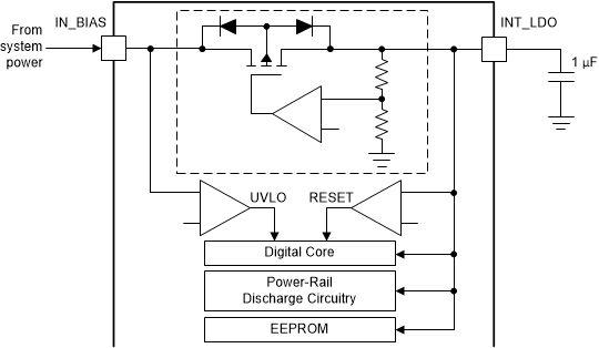
The internal LDO provides a regulated voltage to the internal digital core and analog circuitry. The internal LDO has a nominal output voltage of 2.5 V and can support up to 10 mA of external load.
When system power fails, the UVLO comparator triggers the power-down sequence. If system power drops below , the digital core is reset and all remaining power rails are shut down instantaneously and are pulled low to ground by their internal discharge circuitry (DCDC1-4 and LDO1).
The internal LDO reverse blocks to prevent the discharging of the output capacitor (CINT_LDO) on the INT_LDO pin. The remaining charge on the INT_LDO output capacitor provides a supply for the power rail discharge circuitry to ensure the outputs are discharged to ground even if the system supply has failed. The amount of hold-up time specified in Section 4.5 is a function of the output capacitor value (CINT_LDO) and the amount of external load on the INT_LDO pin, if any. The design allows for enough hold-up time to sufficiently discharge DCDC1-4, and LDO1 to ensure proper processor power-down sequencing.
 Figure 5-9 Internal LDO and UVLO Sensing