SLDS261A November 2019 – February 2021 TPS6521815
PRODUCTION DATA
- 1 Features
- 2 Applications
- 3 Description
- 4 Revision History
- 5 Description (continued)
- 6 Pin Configuration and Functions
- 7 Specifications
-
8 Detailed Description
- 8.1 Overview
- 8.2 Functional Block Diagram
- 8.3
Feature Description
- 8.3.1
Wake-Up and Power-Up and Power-Down Sequencing
- 8.3.1.1 Power-Up Sequencing
- 8.3.1.2 Power-Down Sequencing
- 8.3.1.3 Strobe 1 and Strobe 2
- 8.3.1.4 Supply Voltage Supervisor and Power-Good (PGOOD)
- 8.3.1.5 Backup Supply Power-Good (PGOOD_BU)
- 8.3.1.6 Internal LDO (INT_LDO)
- 8.3.1.7 Current Limited Load Switches
- 8.3.1.8 LDO1
- 8.3.1.9 Coin Cell Battery Voltage Acquisition
- 8.3.1.10 UVLO
- 8.3.1.11 Power-Fail Comparator
- 8.3.1.12 Battery-Backup Supply Power-Path
- 8.3.1.13 DCDC3 and DCDC4 Power-Up Default Selection
- 8.3.1.14 I/O Configuration
- 8.3.1.15 Push Button Input (PB)
- 8.3.1.16 AC_DET Input (AC_DET)
- 8.3.1.17 Interrupt Pin (INT)
- 8.3.1.18 I2C Bus Operation
- 8.3.1
Wake-Up and Power-Up and Power-Down Sequencing
- 8.4 Device Functional Modes
- 8.5 Programming
- 8.6 Register Maps
- 9 Application and Implementation
- 10Power Supply Recommendations
- 11Layout
- 12Device and Documentation Support
- 13Mechanical, Packaging, and Orderable Information
Package Options
Mechanical Data (Package|Pins)
- RSL|48
Thermal pad, mechanical data (Package|Pins)
- RSL|48
Orderable Information
8.5.1 Programming Power-Up Default Values
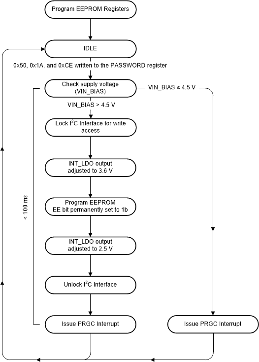
A consecutive write of 0x50, 0x1A, or 0xCE to the password register commits the current register settings to EEPROM memory so they become the new power-up default values.
Only bits marked with (E2) in the register map have EEPROM programmable power-up default settings. All other bits keep the factory settings listed in the register map. Changing the power-up default values is not recommended in production but for prototyping only.
The EEPROM of a device can only be programmed up to 1000 times. The number of programming cycles should never exceed this amount. Contact TI for changing production settings.
EEPROM values can only be changed if the input voltage (VIN_BIAS) is greater than 4.5 V. If the input voltage is less than 4.5 V, EEPROM values remain unchanged and the VPROG interrupt is issued. EEPROM programming requires less than 100 ms. During this time the supply voltage must be held constant and all I2C write commands are ignored. Completion of EEPROM programming is signaled by the EE_CMPL interrupt.
 Figure 8-35 Flow Chart for Programming New
Power-Up Default Values