SLVSCA6C October 2013 – October 2017 TPS65311-Q1
PRODUCTION DATA.
- 1 Features
- 2 Applications
- 3 Description
- 4 Revision History
- 5 Description (continued)
- 6 Pin Configuration and Functions
- 7 Specifications
-
8 Detailed Description
- 8.1 Overview
- 8.2 Functional Block Diagram
- 8.3
Feature Description
- 8.3.1 Buck Controller (BUCK1)
- 8.3.2 Synchronous Buck Converters BUCK2 and BUCK3
- 8.3.3 BOOST Converter
- 8.3.4 Frequency-Hopping Spread Spectrum
- 8.3.5 Linear Regulator LDO
- 8.3.6 Gate Driver Supply
- 8.3.7 RESET
- 8.3.8 Soft Start
- 8.3.9 Power-on Reset Flag
- 8.3.10 WAKE Pin
- 8.3.11 IRQ Pin
- 8.3.12 VBAT Undervoltage Warning
- 8.3.13 VIN Over or Undervoltage Protection
- 8.3.14 External Protection
- 8.3.15 Overtemperature Detection and Shutdown
- 8.3.16 Independent Voltage Monitoring
- 8.3.17 GND Loss Detection
- 8.3.18 Reference Voltage
- 8.3.19 Shutdown Comparator
- 8.3.20 LED and High-Side Switch Control
- 8.3.21 Window Watchdog
- 8.3.22 Timeout in Start-Up Modes
- 8.4 Device Functional Modes
- 8.5 Programming
- 8.6 Register Map
-
9 Application and Implementation
- 9.1 Application Information
- 9.2
Typical Applications
- 9.2.1 Buck Controller (BUCK1)
- 9.2.2 Synchronous Buck Converters BUCK2 and BUCK3
- 9.2.3 BOOST Converter
- 9.2.4 Linear Regulator
- 10Power Supply Recommendations
- 11Layout
- 12Device and Documentation Support
- 13Mechanical, Packaging, and Orderable Information
Package Options
Mechanical Data (Package|Pins)
- RVJ|56
Thermal pad, mechanical data (Package|Pins)
- RVJ|56
Orderable Information
8 Detailed Description
8.1 Overview
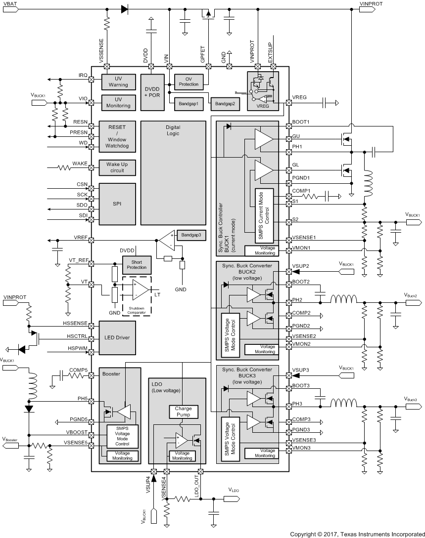
The device includes one high-voltage buck controller for pre-regulation combined with a two-buck and one-boost converter for post regulation. A further integrated low-dropout (LDO) regulator rounds up the power-supply concept and offers a flexible system design with five independent-voltage rails. The device offers a low power state (LPM0 with all rails off) to reduce current consumption in case the system is constantly connected to the battery line. All outputs are protected against overload and over temperature.
An external PMOS protection feature makes the device capable of sustaining voltage transients up to 80 V. This external PMOS is also used in safety-critical applications to protect the system in case one of the rails shows a malfunction (undervoltage, overvoltage, or overcurrent).
Internal soft-start ensures controlled startup for all supplies. Each power-supply output has an adjustable output voltage based on the external resistor-network settings.
8.3 Feature Description
8.3.1 Buck Controller (BUCK1)
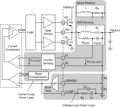
The main buck controller operates using constant frequency peak current mode control. The output voltage is programmable with external resistors.
The switching frequency is set to a fixed value of fSWBUCK1. Peak current-mode control regulates the peak current through the inductor such that the output voltage VBUCK1 is maintained to its set value. Current mode control allows superior line-transient response. The error between the feedback voltage VSENSE1 and the internal reference produces an error signal at the output of the error amplifier (COMP1) which serves as target for the peak inductor current. At S1–S2, the current through the inductor is sensed as a differential voltage and compared with this target during each cycle. A fall or rise in load current produces a rise or fall in voltage at VSENSE1, which causes COMP1 to rise or fall respectively, thus increasing or decreasing the current through the inductor until the average current matches the load. In this way the output voltage VBUCK1 is maintained in regulation.
The high-side N-channel MOSFET is turned on at the beginning of each clock cycle and kept on until the inductor current reaches its peak value as set by the voltage loop. Once the high external FET is turned OFF, and after a small delay (shoot-through delay), the lower N-channel MOSFET is turned on until the start of the next clock cycle. In dropout operation the high-side MOSFET stays on 100%. In every fourth period the duty cycle is limited to 95% in order to charge the bootstrap capacitor at BOOT1. This allows a maximum duty cycle of 98.75%.
The maximum value of COMP1 is clamped so that the maximum current through the inductor is limited to a specified value. The BUCK1 controller output voltage is monitored by a central independent voltage-monitoring circuit, which has an independent voltage-monitoring bandgap reference for safety reasons. In addition, BUCK1 is thermally protected with a dedicated temperature sensor.
8.3.2 Synchronous Buck Converters BUCK2 and BUCK3
Both regulators are synchronous converters operating with a fixed switching frequency ƒsw = 2.45 MHz. For each buck converter, the output voltage is programmable with external resistors. The synchronous operation mode improves the overall efficiency. BUCK3 switches in phase with BUCK1, and BUCK2 switches at a 216-degree shift to BUCK3 to minimize input current ripple.
Each buck converter can provide a maximum current of 2 A and is protected against short circuits to ground. In case of a short circuit to ground, the integrated cycle-by-cycle current limit turns off the high-side FET when its current reaches IHS-Limit and the low-side FET is turned on until the end of the given cycle. When the current limit is reached in the beginning of the cycle for five consecutive cycles, the pulse-width modulation (PWM) is forced low for sixteen cycles to prevent uncontrolled current build-up. In case the low-side current limit of ILS-Limit is reached, for example, because of an output short to the VSUP2 and VSUP23 pins, the low-side FET is turned off until the end of the cycle. If this is detected shortly after the high-low PWM transition (immediately after the low-side overcurrent comparator blanking time), both FETs are turned off for sixteen cycles.
The output voltages of the BUCK2 and BUCK3 regulators are monitored by a central independent voltage-monitoring circuit, which has an independent voltage-monitoring bandgap reference for safety reasons. In addition BUCK2 and BUCK3 are thermally protected with a dedicated temperature sensor.
8.3.3 BOOST Converter
The BOOST converter is an asynchronous converter operating with a fixed switching frequency ƒsw = 2.45 MHz. It switches in phase with BUCK1. At low load, the boost regulator switches to pulse skipping.
The output voltage is programmable with external resistors.
The internal low-side switch can handle maximum 1-A current, and is protected with a current limit. In case of an overcurrent, the integrated cycle-by-cycle current limit turns off the low-side FET when its current reaches ICLBOOST until the end of the given cycle. When the current limit is reached in the beginning of the cycle for five consecutive cycles, the PWM is forced low for sixteen cycles to prevent uncontrolled current build-up.
The BOOST converter output voltage is monitored by a central independent voltage-monitoring circuit, which has an independent voltage-monitoring bandgap reference for safety reasons. If the VMONTH_L > VSENSE5 or VSENSE5 > VMONTH_H, the output is switched off and the BOOST_FAIL bit in the SPI PWR_STAT register is set. The BOOST can be reactivated by setting BOOST_EN bit in the PWR_CONFIG register.
In addition, the BOOST converter is thermally protected with a dedicated temperature sensor. If TJ > TOTTH, the BOOST converter is switched off and bit OT_BOOST in PWR_STAT register is set. Reactivation of the booster is only possible if the OT_BOOST bit is 0, and the booster enable bit in the PWR_CONFIG register is set to 1.
8.3.4 Frequency-Hopping Spread Spectrum
The TPS65311-Q1 features a frequency-hopping pseudo-random spectrum or triangular spreading architecture. The pseudo-random implementation uses a linear feedback shift register that changes the frequency of the internal oscillator based on a digital code. The shift register is designed in such a way that the frequency shifts only by one step at each cycle to avoid large jumps in the buck and boost switching frequencies. The triangular function uses an up-down counter. Whenever spread spectrum is enabled (SPI command), the internal oscillator frequency is varied from one BUCK1 cycle to the next within a band of 0.8 x fOSC ... fOSC from a total of 16 different frequencies. This means that BUCK3 and BOOST also step through 16 frequencies. The internal oscillator can also change its frequency during the period of BUCK2, yielding a total of 31 frequencies for BUCK2.
8.3.5 Linear Regulator LDO
The LDO is a low drop out regulator with an adjustable output voltage through an external resistive divider network. The output has an internal current-limit protection in case of an output overload or short circuit to ground. In addition, the output is protected against overtemperature. If TJ > TOTTH, the LDO is switched off and bit OT_LDO in PWR_STAT register is set. Reactivation of the LDO is only possible through the SPI by setting the LDO enable bit in the PWR_CONFIG register to 1 if the OT_LDO bit is 0.
The LDO output voltage is monitored by a central independent voltage-monitoring circuit, which has an independent voltage-monitoring bandgap reference for safety reasons. If the VMONTH_L > VSENSE4 or VSENSE4 > VMONTH_H, the output is switched off and the LDO_FAIL bit in the SPI PWR_STAT register is set. The LDO can be reactivated through the SPI by setting the LDO_EN bit in the PWR_CONFIG register. In case of overvoltage in VTCHECK and RAMP mode, the GPFET is turned off and the device changes to ERROR mode.
8.3.6 Gate Driver Supply
The gate drivers of the BUCK1 controller, BUCK2 and BUCK3 converters and the BOOST converter are supplied from an internal linear regulator. The internal linear regulator output (5.8-V typical) is available at the VREG pin and must be decoupled using a typical 2.2-μF ceramic capacitor. This pin has an internal current-limit protection and must not be used to power any other circuits.
The VREG linear regulator is powered from VINPROT by default when the EXTSUP voltage is less than 4.6 V (typical).
If the VINPROT is expected to go to high levels, there can be excessive power dissipation in this regulator when using large external MOSFETs. In this case, it is advantageous to power this regulator from the EXTSUP pin, which can be connected to a supply less than VINPROT but high enough to provide the gate drive. When EXTSUP is connected to a voltage greater than 4.8 V, the linear regulator automatically switches to EXTSUP as its input to provide this advantage. This automatic switch-over to EXTSUP can only happen once the TPS65311-Q1 device reaches ACTIVE mode. Efficiency improvements are possible when one of the switching regulator rails from the TPS65311-Q1, or any other voltage available in the system is used to power EXTSUP. The maximum voltage that must be applied to EXTSUP is 12 V.
8.3.7 RESET
RESN and PRESN are open drain outputs which are active if one or more of the conditions listed in Table 1 are valid. RESN active (low) is extended for tRESNHOLD after a reset is triggered. RESN is the main processor reset and also asserts PRESN as a slave signal.
PRESN is latched and is released when window trigger mode of the watchdog is enabled (first rising edge at the WD pin).
RESN and PRESN must keep the main processor and peripheral devices in a defined state during power up and power down in case of improper supply voltages or a critical failure condition. Therefore, for low supply voltages the topology of the reset outputs specify that RESN and PRESN are always held at a low level when RESN and PRESN are asserted, even if VIN falls below VPOR or the device is in SHUTDOWN mode.
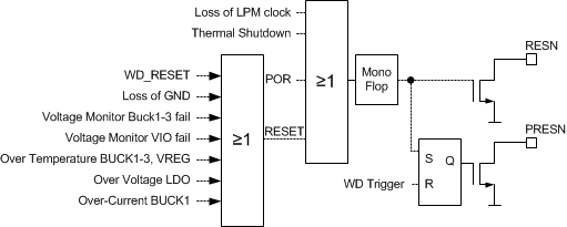 Figure 17. RESET Functionality
Table 1. Reset Conditions
| RESET CONDITION | CONSEQUENCE FOR DEVICE |
|---|---|
| POR, Loss of LPM Clock, and Thermal Shutdown | The device reinitializes all registers with their default values. Error counter is cleared. |
| Voltage Monitor BUCK 1-3 | Input voltage at VMON1-3 pin out-of-bounds: VVMON1-3 < VMONTH_L or VVMON1-3 > VMONTH_H |
| Over Voltage LDO | Vsense4 > VMONTH_H |
| Voltage Monitor VIO | Input voltage at VIO pin out-of-bounds: VVIO < VVIOMON TH |
| Loss of GND | Open at PGNDx or GND pin |
| OT BUCK1, BUCK2, BUCK3, VREG | Overtemperature on BUCK1–3 or VREG |
| WD_RESET | Watchdog window violation |
Any reset event (without POR, thermal shutdown, or loss of LPM clock) increments the error counter (EC) by one. After a reset is consecutively triggered NRES times, the device transfers to the LPM0 state, and the EC is reset to 0. The counter is decremented by one if an SPI LPM0_CMD is received. Alternatively, the device can be put in LOCK state once an SPI LOCK_CMD is received. Once the device is locked, it cannot be activated again by a wake condition. The reset counter and lock function avoid cyclic start-up and shut-down of the device in case of a persistent fault condition. The reset counter content is cleared with a POR condition, a thermal shutdown or a loss of LPM clock. Once the device is locked, a voltage below VPOR at VIN pin or a thermal shutdown condition are the only ways to unlock the device.
8.3.8 Soft Start
The output voltage slopes of BUCK, BOOST and LDO regulators are limited during ramp-up (defined by tSTARTx). During this period the target output voltage slowly settles to its final value, starting from 0 V. In consequence, regulators that offer low-side transistors (BUCK1, BUCK2 and BUCK3) actively discharge their output rails to the momentary ramp-value if previously charged to a higher value.
8.3.9 Power-on Reset Flag
The POR flag in the SYS_STAT SPI register is set:
- When VIN is below the VPOR threshold
- System is in thermal shutdown
- Over or undervoltage on DVDD
- Loss of low power clock
8.3.10 WAKE Pin
Only when the device is in LPM0 mode, it can be activated by a positive voltage on the WAKE pin with a minimum pulse width tWAKE. A valid wake condition is latched. Normal deactivation of the device can only occur through the SPI Interface by sending an SPI command to enter LMP0. Once in LMP0, the device stays in LPM0 when the WAKE pin is low, or restarts to TESTSTART when the WAKE pin is high.
The WAKE pin has an internal pulldown resistance RPD-WAKE, and the voltage on the pin is not allowed to exceed 60 V. A higher voltage compliance level in the application can be achieved by applying an external series resistor between the WAKE pin and the external wake-up signal.
The device cannot be re-enabled by toggling the WAKE pin when the device is in LOCKED state (by SPI command).
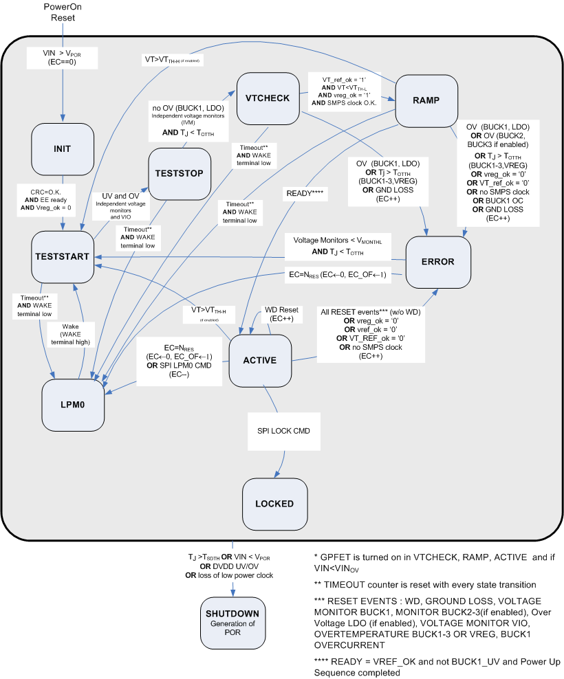 Figure 18. Operating Mode Transitions
8.3.11 IRQ Pin
The IRQ pin has two different functions. In OPERATING mode, the pin is forced low when the voltage on the battery line is below the VSSENSETHx threshold. The IRQ pin is low as long as PRESN is low. If PRESN goes high and the battery line is already below the VSSENSETHx threshold, the IRQ pin is forced high for tVSSENSE_BLK.
8.3.12 VBAT Undervoltage Warning
- Low battery condition on VSSENSE asserts IRQ output (interrupt for µC, open drain output)
- Sense input can be directly connected to VBAT through the resistor
- Detection threshold for undervoltage warning can be selected through the SPI.
- An integrated filter time avoids false reaction due to spikes on the VBAT line.
8.3.13 VIN Over or Undervoltage Protection
- Undervoltage is monitored on the VIN line, for POR generation.
- Two VIN overvoltage shutdown thresholds (VOVTH) can be selected through the SPI. After POR, the lower threshold is enabled.
- During LPM0, only the POR condition is monitored.
- An integrated filter time avoids false reaction due to spikes on the VIN line.
- In case of overvoltage, the external PMOS is switched off to protect the device. The BUCK1 controller is not switched off and it continues to run until the undervoltage on VREG or BUCK1 output is detected.
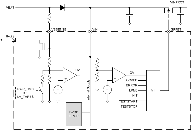 Figure 19. Overvoltage or Undervoltage Detection Circuitry
8.3.14 External Protection
The external PMOS switch is disabled if:
- The device detects VIN overvoltage
- The device is in ERROR, LOCKED, POR, INIT, TESTSTART, TESTSTOP or LPM0 mode
NOTE
Depending on the application, the external PMOS may be omitted as long as
VBAT < 40 V
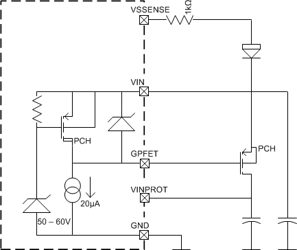 Figure 20. PMOS Control Circuitry
8.3.15 Overtemperature Detection and Shutdown
There are two levels of thermal protection for the device.
Overtemperature is monitored locally on each regulator.
-
OT for BUCK1, BUCK2, and BUCK3 If a thermal monitor on the buck rails reaches a threshold higher than TOTTH, the device enters ERROR mode. Leaving ERROR mode is only possible if the temperature is below TOTTH–TOTHY.
-
OT for BOOST and LDO If the temperature monitor of the boost or the LDO reaches the TOTTH threshold, the corresponding regulator is switched off.
-
Overtemperature Shutdown is monitored on a central die position. In case the TSDTH is reached, the device enters shutdown mode. It leaves shutdown when the TSD sensor is below TSDTH – TSDHY. This event internally generates a POR.
8.3.16 Independent Voltage Monitoring
The device contains independent voltage-monitoring circuits for BUCK1–3, LDO, VIO and BOOST. The reference voltage for the voltage monitoring unit is derived from an independent bandgap. BUCKs 1–3 use separate input pins for monitoring. The monitoring circuit is implemented as a window comparator with an upper and lower threshold.
If there is a violation of the upper (only LDO [RAMP, VTCHECK], or BUCK1–3) or lower threshold (only BUCK1–3, or VIO), the device enters ERROR mode, RESN and PRESN are asserted low, the external PMOS (main system switch) is switched off, and the EC is incremented.
In TESTSTART mode, a self-test of the independent voltage monitors is performed.
In case any of the supply rails for BUCK2, BUCK3, LDO or BOOST are not used in the application, the respective VMON2 and VMON3 or VSENSE4 and VSENSE5 pin of the unused supply must be connected to VMON1. Alternatively, the VSENSE4 pin can also be connected directly to ground in case the LDO is not used.
8.3.17 GND Loss Detection
All power grounds PGNDx are monitored. If the voltage difference to GND exceeds VGLTH-low or VGLTH-high, the device enters ERROR mode. RESN and PRESN are asserted low, the external PMOS (main system switch) is switched off, and the EC is incremented.
8.3.18 Reference Voltage
The device includes a precise voltage reference output to supply a system ADC. If this reference voltage is used in the application, a decoupling capacitor between 0.6 and 5 µF must be used. If this reference voltage is not used in the application, this decoupling capacitor can be left out. The VREF output is enabled in RAMP state. The output is protected against a short to GND.
8.3.19 Shutdown Comparator
An auxiliary, short circuit protected output supplied from DVDD is provided at the VT_REF pin. This output is used as a reference for an external resistive divider to the VT pin. In case a voltage > VTTH is detected on the VT pin, the main switch (external PMOS driven by GPFET) is switched off. This functionality can be used to monitor over and under temperature (using a NTC resistor) to avoid operation below or above device specifications.
If the voltage at VT_REF falls below VVT_REF SH while the shutdown comparator is enabled, an ERROR transition occurs. The shutdown comparator is enabled in VTCHECK state, and can be turned off by SPI. Disabling the comparator saves power by also disabling the VT_REF output.
8.3.20 LED and High-Side Switch Control
This module controls an external PMOS in current-limited high-side switch.
The current levels can be adjusted with an external sense resistor. Enable and disable is done with the HS_EN bit. The switch is controlled by the HSPWM input pin. Driving HSPWM high turns on the external FET.
The device offers an open load diagnostic indicated by the HS_OL flag in the SPI register PWR_STAT. Open load is also indicated in case the voltage on VINPROT–VSSENSE does not drop below the threshold when PWM is low (self-test).
A counter monitors the overcurrent condition to detect the risk of overheating. While HSPWM = high and HS_EN = high the counter is incremented during overcurrent conditions, and decremented if the current is below the overcurrent threshold at a sampling interval of tS HS (see Figure 22). When reaching a net current limit time of tHSS CL, the driver is turned off and the HS_EN bit is cleared. This feature can be disabled by SPI bit HS_CLDIS. When HS_EN is cleared, the counter is reset.
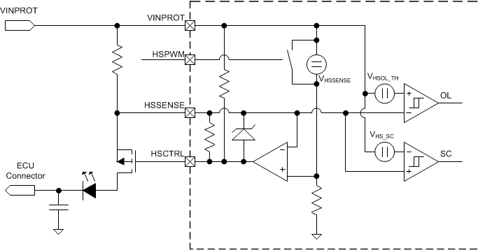 Figure 21. High-Side Control Circuit
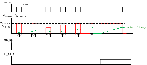 Figure 22. HS Overcurrent Counter
NOTE
In case the LED or high-side switch control is not used in the application, HSSENSE must be connected to VINPROT.
8.3.21 Window Watchdog
The WD is used to detect a malfunction of the MCU and DSP. Description:
- Timeout trigger mode with long timing starts on the rising edge at RESN
- Window trigger mode with fixed timing after the first and each subsequent rising edge at the WD pin
- Watchdog is triggered by rising edge at the WD pin
A watchdog reset happens by:
- A trigger pulse outside the WD trigger open window
- No trigger pulse during window time
After the RESN pin is released (rising edge) the DSP and MCU must trigger the WD by a rising edge on the WD pin within a fixed time ttimeout. With this first trigger, the window watchdog functionality is released.
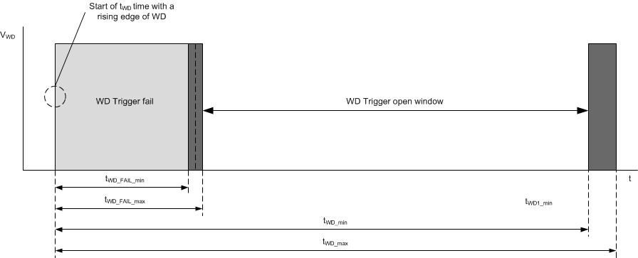 Figure 23. WD Window Description
8.3.22 Timeout in Start-Up Modes
A timer is used to limit the time during which the device can stay in each of the start-up modes: TESTSTART, TESTSTOP, VTCHECK and RAMP. If the device enters one of these start-up modes and VIN or VT is not in a proper range, the part enters LPM0 after ttimeout is elapsed and the WAKE pin is low.
8.4 Device Functional Modes
8.4.1 Operating Modes
8.4.1.1 INIT
Coming from a power-on reset the device enters INIT mode. The configuration data from the EEPROM is loaded in this mode. If the checksum is valid and the internal VREG monitor is indicating an undervoltage condition (self-test VREG comparator), the device enters TESTSTART.
8.4.1.2 TESTSTART
TESTSTART mode is entered:
- After the INIT state (coming from power on)
- After detecting that VT > VTTH-H
- After ERROR mode and the fail condition is gone
- After a wake command in LPM0
In this mode the OV and UV comparators of BUCK1, BUCK2, BUCK3, BOOST, LDO and VIO are tested. The test is implemented in such a way that during this mode all comparators have to deliver a 1 (fail condition). If this is the case the device enters TESTSTOP mode.
If this is not the case, the device stays in TESTSTART. If the WAKE pin is low, the device enters LPM0 after ttimeout. If the pin WAKE is high, the part stays in TESTSTART.
8.4.1.3 TESTSTOP
In this mode the OV and UV comparators are switched to normal operation. It is expected that only the UV comparators give a fail signal. In case there is an OV condition on any rail or one of the rails has an overtemperature the device stays in TESTSTOP. If the WAKE pin is low the device enters LPM0 mode after ttimeout. If the WAKE pin is high, the part stays in TESTSTOP. If there is no overvoltage and overtemperature detected, the part enters VTCHECK mode.
8.4.1.4 VTCHECK
VTCHECK mode is used to:
- Switch on external GPFET in case VIN < VOVTH_L
- Turn on VREG regulator and VT_REF
- Check if voltage on pin VT < VTTH-L
- Check if SMPS clock is running correctly
- Check if VREG,VT_REF exceed the minimum voltage
If all checks are valid the part enters the RAMP state. In case the device is indicating a malfunction and the WAKE pin is low, the device enters LPM0 after ttimeout to reduce current consumption.
In case the voltage monitors detect an overvoltage condition on BUCK1, BUCK2, BUCK3, or LDO, a loss of GND or an overtemperature condition on BUCK1, BUCK2, BUCK3, or VREG the device enters ERROR mode and the error counter is increased.
8.4.1.5 RAMP
In this mode the device runs through the power-up sequencing of the SMPS rails (see Figure 24).
8.4.1.5.1 Power-Up Sequencing
After the power-up sequence (see Figure 24), all blocks are fully functional. BUCK1 starts first. After tSEQ2 elapses and BUCK1 is above the undervoltage threshold, BUCK2 and BOOST start. BUCK3 and VREF start one tSEQ1 after BUCK2. After the release of RESN pin, the µC can enable the LDO per SPI by setting bit 4 LDO_EN in PWR_CONFIG register to 1 (per default, this LDO_EN is set to 0 after each reset to the µC).
In case any of the following conditions occurduring power-up sequencing, the device enters ERROR mode and the error counter (EC) is increased:
- Overtemperature on BUCK1, BUCK2, BUCK3 or VREG
- Overvoltage on BUCK1, BUCK2, BUCK3 or LDO
- Overcurrent on BUCK1
- SMPS clock fail
- VT_REF and VREG undervoltage
- Loss of GND
In case VT > VTTH-H, the device transitions to TESTSTART.
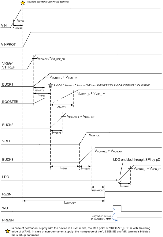 Figure 24. Power-up Sequencing
After the power-up sequence is completed (except LDO) without detecting an error condition, the device enters ACTIVE mode.
8.4.1.5.2 Power-Down Sequencing
There is no dedicated power-down sequencing. All rails are switched off at the same time. The external FETs of BUCK1 are switched off and the outputs of BUCK2, BUCK3, BOOST (PHx) and the LDO are switched in a high-impedance state.
8.4.1.6 ACTIVE
This is the normal operating mode of the device. Transitions to other modes:
→ ERROR
The device is forced to go to ERROR in case of:
- Any RESET event (without watchdog reset)
- VREG, VREF, or VT_REF below undervoltage threshold
- SMPS clock fail
During the transition to ERROR mode the EC is incremented.
→ LOCKED
In case a dedicated SPI command (SPI_LOCK_CMD) is issued.
→ TESTSTART
The device moves to TESTSTART after detecting that VT < VTTH-L.
→ LPM0
The device can be forced to enter LPM0 with a SPI LPM0 command. During this transition the EC is decremented.
If the EC reaches the NRES value, the device transitions to LPM0 mode and EC is cleared. Depending on the state of the WAKE pin, the device remains in LMP0 (WAKE pin low) or restart to TESTSTART (WAKE pin high). To indicate the device entered LPM0 after EC reached NRES value, a status bit EC_OF (error counter overflow, SYS_STAT bit 3) is set. The EC_OF bit is cleared on read access to the SYS_STAT register.
A watchdog reset in ACTIVE mode only increases the EC, but it does not change the device mode.
8.4.1.7 ERROR
In this mode all power stages and the GPFET are switched off. The devices leave ERROR mode and enter TESTSTART if:
- All rails indicate an undervoltage condition
- No GND loss is detected
- No overtemperature condition is detected
When the EC reaches the NRES value, the device transitions to LPM0 and the EC is cleared. To indicate the device entered LPM0 after EC reached NRES, a status bit EC_OF (error counter overflow, SYS_STAT bit 3) is set. The EC_OF bit is cleared on read access to the SYS_STAT register.
8.4.1.8 LOCKED
Entering this mode disables the device. The only way to leave this mode is through a power-on reset, thermal shutdown, or the loss of an LPM clock.
8.4.1.9 LPM0
Low-power mode 0 is used to reduce the quiescent current of the system when no functionality is needed. In this mode the GPFET and all power rails except for DVDD are switched off.
In case a voltage > VWAKE_ON longer than tWAKE is detected on the WAKE pin, the part switches to TESTSTART mode.
8.4.1.10 SHUTDOWN
The device enters and stays in this mode, as long as TJ > TSDTH - TSDHY or VIN < VPOR or DVDD under or overvoltage, or loss of low power clock is detected. Leaving this mode and entering INIT mode generates an internal POR.
8.5 Programming
8.5.1 SPI
The SPI provides a communication channel between the TPS65311-Q1 and a controller. The TPS65311-Q1 is always the slave. The controller is always the master. The SPI master selects the TPS65311-Q1 by setting CSN (chip select) to low. SDI (slave in) is the data input, SDO (slave out) is the data output, and SCK (serial clock input) is the SPI clock provided by the master. If chip select is not active (high), the data output SDO is high impedance. Each communication consist of 16 bits.
1 bit parity (odd) (parity is built over all bits including: R/W, CMD_ID[5:0], DATA[7:0])
1 bit R/W; read = 0 and write = 1
6 bits CMD identifier
8 bits data
 Figure 25. SPI Bit-Frame
Each command is valid if:
- A valid CMD_ID is sent
- The parity bit (odd) is correct
- Exactly 16 SPI clocks are counted between falling and rising edge of CSN
The response to each master command is given in the following SPI cycle. The response address is the CMD_ID of the previous sent message and the corresponding data byte. The response data is latched with the previous cycle such that a response to a write command is the status of the register before the write access. (Same response as a read access.) The response to an invalid command is the original command with the correct parity bit. The response to an invalid number of SPI clock cycles is a SPI_SCK_FAIL communication (CMD_ID = 0x03). Write access to a read-only register is not reported as an SPI error and is treated as a read access. The initial answer after the first SPI command sent is: CMD_ID[5:0] = 0x3F and Data[7:0] 0x5A.
8.5.1.1 FSI Bit
The slave transmits an FSI bit between the falling edge of CSN and the rising edge of SCK. If the SDO line is high during this time, a failure occurred in the system and the MCU must use the PWR_STAT to get the root cause. A low level of SDO indicates normal operation of the device.
The FSI bit is set when: PWR_STAT ! = 0x00, or (SYS_STAT and 0x98) ! = 0x00, or SPI_STAT ! = 0x00. The FSI is cleared when all status flags are cleared.
8.6 Register Map
| CMD_ID | NAME | Bit7 | Bit6 | Bit5 | Bit4 | Bit3 | Bit2 | Bit1 | Bit0 |
|---|---|---|---|---|---|---|---|---|---|
| 0x00 | NOP | 0x00 | |||||||
| 0x03 | SPI_SCK_FAIL | 1 | 0 | 0 | SCK_OF | SCK[3] | SCK[2] | SCK[1] | SCK[0] |
| 0x11 | LPM0_CMD | 0xAA | |||||||
| 0x12 | LOCK_CMD | 0x55 | |||||||
| 0x21 | PWR_STAT | BUCK_FAIL | VREG_FAIL | OT_BUCK | OT_LDO | OT_BOOST | LDO_FAIL | BOOST_FAIL | HS_OL |
| 0x22 | SYS_STAT | WD | POR | TestMode | SMPCLK_FAIL | EC_OF | EC2 | EC1 | EC0 |
| 0x23 | SPI_STAT | CLOCK_FAIL | CMD_ID FAIL | PARITY FAIL | |||||
| 0x24 | COMP_STAT | BUCK3-1 | BUCK3-0 | BUCK2-1 | BUCK2-0 | ||||
| 0x29 | Serial Nr 1 | Bit [7:0] | |||||||
| 0x2A | Serial Nr 2 | Bit [15:8] | |||||||
| 0x2B | Serial Nr 3 | Bit [23:16] | |||||||
| 0x2C | Serial Nr 4 | Bit [31:24] | |||||||
| 0x2D | Serial Nr 5 | Bit [39:32] | |||||||
| 0x2E | Serial Nr 6 | Bit [47:40] | |||||||
| 0x2F | DEV_REV | Major3 | Major2 | Major1 | Major0 | Minor3 | Minor2 | Minor1 | Minor0 |
| 0x31 | PWR_CONFIG | BUCK2_EN | BUCK3_EN | LDO_EN | BOOST_EN | HS_EN | GPFET_OV_HIGH | IRQ_THRES | |
| 0x32 | DEV_CONFIG | HL_CLDIS | VT_EN | RSV | RSV | ||||
| 0x33 | CLOCK_CONFIG | F_EN | SS_EN | SS_MODE | F4 | F3 | F2 | F1 | F0 |
8.6.1 Register Description
| NOP 0x00 | ||||||||
|---|---|---|---|---|---|---|---|---|
| Bit7 | Bit6 | Bit5 | Bit4 | Bit3 | Bit2 | Bit1 | Bit0 | |
| After RESET | 0 | 0 | 0 | 0 | 0 | 0 | 0 | 0 |
| Read | 0 | 0 | 0 | 0 | 0 | 0 | 0 | 0 |
| Write | d.c. | d.c. | d.c. | d.c. | d.c. | d.c. | d.c. | d.c. |
| SPI_SCK_FAIL 0x03 | ||||||||
|---|---|---|---|---|---|---|---|---|
| Bit7 | Bit6 | Bit5 | Bit4 | Bit3 | Bit2 | Bit1 | Bit0 | |
| Default after RESET | 1 | 0 | 0 | 0 | 0 | 0 | 0 | 0 |
| Read | 1 | 0 | 0 | SCK_OF | SCK[3] | SCK[2] | SCK[1] | SCK[0] |
| Write | d.c. | d.c. | d.c. | d.c. | d.c. | d.c. | d.c. | d.c. |
| BIT NAME | BIT NO. | DESCRIPTION | |
|---|---|---|---|
| SCK_OF | 4 | Between a falling and a rising edge of CSN, the number of SCK was greater than 16. | |
| 0: | |||
| 1: | Number of SCK cycles was > 16 | ||
| Comment: This flag is cleared after its content is transmitted to the master. | |||
| BIT NAME | BIT NO. | DESCRIPTION | |
|---|---|---|---|
| SCK[3:0] | 3:0 | The number of rising edges on SCK between a falling and a rising edge of CSN minus 1. Saturates at 0xF if 16 or more edges are received. | |
| Comment: This flag is cleared after its content is transmitted to the master. | |||
| LPM0_CMD 0x11 | ||||||||
|---|---|---|---|---|---|---|---|---|
| Bit7 | Bit6 | Bit5 | Bit4 | Bit3 | Bit2 | Bit1 | Bit0 | |
| After RESET | 0 | 0 | 0 | 0 | 0 | 0 | 0 | 0 |
| Read | 0 | 0 | 0 | 0 | 0 | 0 | 0 | 0 |
| Write | 0xAA | |||||||
| This command is used to send the device into LPM0 mode. | ||||||||
| LOCK_CMD 0x12 | ||||||||
|---|---|---|---|---|---|---|---|---|
| Bit7 | Bit6 | Bit5 | Bit4 | Bit3 | Bit2 | Bit1 | Bit0 | |
| After RESET | 0 | 0 | 0 | 0 | 0 | 0 | 0 | 0 |
| Read | 0 | 0 | 0 | 0 | 0 | 0 | 0 | 0 |
| Write | 0x55 | |||||||
| Sending a lock command (0x55) brings the device into LOCK mode. Only a POR brings the device out of this state. | ||||||||
| PWR_STAT 0x21 | ||||||||
|---|---|---|---|---|---|---|---|---|
| Bit7 | Bit6 | Bit5 | Bit4 | Bit3 | Bit2 | Bit1 | Bit0 | |
| Default after POR | 0 | 0 | 0 | 0 | 0 | 0 | 0 | 0 |
| Read | BUCK_FAIL | VREG_FAIL | OT_BUCK | OT_LDO | OT_BOOST | LDO_FAIL | BOOST_FAIL | HS_OL |
| Write | d.c. | d.c. | d.c. | d.c. | d.c. | d.c. | d.c. | d.c. |
| BIT NAME | BIT NO. | DESCRIPTION | |
|---|---|---|---|
| BUCK_FAIL | 7 | BUCK power fail flag | |
| 0: | |||
| 1: | Power stages shutdown detected caused by OC BUCK1, UV, OV, loss of GND (BOOST + all bucks) | ||
| BUCK_FAIL flag is cleared in case the fail condition is not present anymore and the flag is transmitted to the master. | |||
| BIT NAME | BIT NO. | DESCRIPTION | |
|---|---|---|---|
| VREG_FAIL | 6 | Internal voltage regulator too low | |
| 0: | |||
| 1: | VREG fail | ||
| VREG_FAIL flag is cleared in case the fail condition is not present anymore and the flag is transmitted to the master. | |||
| BIT NAME | BIT NO. | DESCRIPTION | |
|---|---|---|---|
| OT_BUCK | 5 | BUCK1-3 overtemperature flag | |
| 0: | |||
| 1: | IC power stages shutdown due to overtemperature | ||
| OT flag is cleared in case the fail condition is not present anymore and the flag is transmitted to the master. | |||
| BIT NAME | BIT NO. | DESCRIPTION | |
|---|---|---|---|
| OT_LDO | 4 | LDO overtemperature flag | |
| 0: | |||
| 1: | LDO shutdown due to overtemperature | ||
| OT flag is cleared in case the fail condition is not present anymore and the flag is transmitted to the master. | |||
| BIT NAME | BIT NO. | DESCRIPTION | |
|---|---|---|---|
| OT_BOOST | 3 | Boost overtemperature flag | |
| 0: | |||
| 1: | BOOST shutdown due to overtemperature | ||
| OT flag is cleared in case the fail condition is not present anymore and the flag is transmitted to the master. | |||
| BIT NAME | BIT NO. | DESCRIPTION | |
|---|---|---|---|
| LDO_FAIL | 2 | LDO under or overvoltage flag | |
| 0: | |||
| 1: | LDO out of regulation | ||
| LDO_FAIL flag is cleared if there is no undervoltage and no overvoltage and the flag is transmitted to the master. | |||
| BIT NAME | BIT NO. | DESCRIPTION | |
|---|---|---|---|
| BOOST_FAIL | 1 | Booster under or overvoltage flag or loss of GND | |
| 0: | |||
| 1: | Booster out of regulation | ||
| BOOST_FAIL flag is cleared if there is no undervoltage and no overvoltage and the flag was transmitted to the master. | |||
| BIT NAME | BIT NO. | DESCRIPTION | |
|---|---|---|---|
| HS_OL | 0 | High-side switch open load condition | |
| 0: | |||
| 1: | Open load at high side | ||
| Bit indicates current OL condition of high side (no flag) | |||
| SYS_STAT 0x22 | ||||||||
|---|---|---|---|---|---|---|---|---|
| Bit7 | Bit6 | Bit5 | Bit4 | Bit3 | Bit2 | Bit1 | Bit0 | |
| Default after POR | 0 | 0 | 0 | 0 | 0 | 0 | 0 | 1 |
| Read | WD | POR | Testmode | SMPCLK_FAIL | 0 | EC2 | EC1 | EC0 |
| Write | d.c. | d.c. | d.c. | d.c. | d.c. | d.c. | d.c. | d.c. |
| BIT NAME | BIT NO. | DESCRIPTION | |
|---|---|---|---|
| WD | 7 | Watchdog reset flag | |
| 0: | |||
| 1: | Last reset caused by watchdog | ||
| Comment: This flag is cleared after its content is transmitted to the master. | |||
| BIT NAME | BIT NO. | DESCRIPTION | |
|---|---|---|---|
| POR | 6 | Power-on reset flag | |
| 0: | |||
| 1: | Last reset caused by a POR condition | ||
| Comment: This flag is cleared after its content is transmitted to the master. | |||
| BIT NAME | BIT NO. | DESCRIPTION | |
|---|---|---|---|
| Testmode | 5 | If this bit is set, the device entered test mode | |
| 0: | |||
| 1: | Device in Testmode | ||
| Comment: This flag is cleared after its content is transmitted to the master and the device left the test mode. | |||
| BIT NAME | BIT NO. | DESCRIPTION | |
|---|---|---|---|
| SMPCLK_ FAIL |
4 | If this bit is set, the clock of the switch mode power supplies is too low. | |
| 0: | Clock OK | ||
| 1: | Clock fail | ||
| Comment: This flag is cleared after its content is transmitted to the master. | |||
| BIT NAME | BIT NO. | DESCRIPTION | |
|---|---|---|---|
| EC [2:0] | 0-2 | Actual error flag counter | |
| 0: | - | ||
| 1: | - | ||
| *Error Counter is only deleted with a POR | |||
| SPI_STAT 0x23 | ||||||||
|---|---|---|---|---|---|---|---|---|
| Bit7 | Bit6 | Bit5 | Bit4 | Bit3 | Bit2 | Bit1 | Bit0 | |
| Default after RESET | 0 | 0 | 0 | 0 | 0 | 0 | 0 | 0 |
| Read | 0 | 0 | 0 | 0 | 0 | CLOCK_FAIL | CMD_ID FAIL | PARITY FAIL |
| Write | d.c. | d.c. | d.c. | d.c. | d.c. | d.c. | d.c. | d.c. |
| BIT NAME | BIT NO. | DESCRIPTION | |
|---|---|---|---|
| CLOCK_FAIL | 2 | Between a falling and a rising edge of CSN, the number of SCK does not equal 16 | |
| 0: | |||
| 1: | Wrong SCK | ||
| Comment: This flag is cleared after its content is transmitted to the master. | |||
| BIT NAME | BIT NO. | DESCRIPTION | |
|---|---|---|---|
| CMD_ID FAIL | 1 | Last received CMD_ID in a reserved area | |
| 0: | |||
| 1: | Wrong CMD_ID | ||
| Comment: This flag is cleared after its content is transmitted to the master and is not set if the number of SCK cycles is incorrect. | |||
| BIT NAME | BIT NO. | DESCRIPTION | |
|---|---|---|---|
| PARITY_FAIL | 0 | Last received command has a parity bit failure | |
| 0: | |||
| 1: | Parity bit error | ||
| Comment: This flag is cleared after its content is transmitted to the master and is not set if the number of SCK cycles is incorrect. | |||
| COMP_STAT 0x24 | ||||||||
|---|---|---|---|---|---|---|---|---|
| Bit7 | Bit6 | Bit5 | Bit4 | Bit3 | Bit2 | Bit1 | Bit0 | |
| Default after RESET | 0 | 0 | 0 | 0 | 0 | 1 | 1 | 0 |
| Read | 0 | 0 | 0 | 0 | BUCK3-1 | BUCK3-0 | BUCK2-1 | BUCK2-0 |
| Write | d.c. | d.c. | d.c. | d.c. | d.c. | d.c. | d.c. | d.c. |
| Register to read back the actual BUCK2/3 compensation settings on COMP2/3. 0x1 ≥ 0 V 0 x 2 ≥ VREG 0 x 3 ≥ open | ||||||||
| DEV_REV 0x2F | ||||||||
|---|---|---|---|---|---|---|---|---|
| Bit7 | Bit6 | Bit5 | Bit4 | Bit3 | Bit2 | Bit1 | Bit0 | |
| After RESET | Major3 | Major2 | Major1 | Major0 | Minor3 | Minor2 | Minor1 | Minor0 |
| Read | Major3 | Major2 | Major1 | Major0 | Minor3 | Minor2 | Minor1 | Minor0 |
| Write | d.c. | d.c. | d.c. | d.c. | d.c. | d.c. | d.c. | d.c. |
| Hard coded device revision can be read from this register | ||||||||
| PWR_CONFIG 0x31 | ||||||||
|---|---|---|---|---|---|---|---|---|
| Bit7 | Bit6 | Bit5 | Bit4 | Bit3 | Bit2 | Bit1 | Bit0 | |
| Default after RESET | 0 | 1 | 1 | 0 | 1 | 0 | 0 | 0 |
| Read | 0 | BUCK2_EN | BUCK3_EN | LDO_EN | BOOST_EN | HS_EN | GPFET_OV_HIGH | IRQ_THRES |
| Write | 0 | BUCK2_EN | BUCK3_EN | LDO_EN | BOOST_EN | HS_EN | GPFET_OV_HIGH | IRQ_THRES |
| This register contains all power rail enable bits. | ||||||||
| BIT NAME | BIT NO. | DESCRIPTION | |
|---|---|---|---|
| BUCK2_EN | 6 | BUCK2 enable flag | |
| 0: | |||
| 1: | Enable BUCK2 | ||
| After reset, BUCK2 is enabled | |||
| BIT NAME | BIT NO. | DESCRIPTION | |
|---|---|---|---|
| BUCK3_EN | 5 | BUCK3 enable flag | |
| 0: | |||
| 1: | Enable BUCK3 | ||
| After reset, BUCK3 is enabled | |||
| BIT NAME | BIT NO. | DESCRIPTION | |
|---|---|---|---|
| LDO_EN | 4 | LDO enable flag | |
| 0: | |||
| 1: | LDO enabled | ||
| After reset, LDO is disabled | |||
| BIT NAME | BIT NO. | DESCRIPTION | |
|---|---|---|---|
| BOOST_EN | 3 | BOOST enable | |
| 0: | |||
| 1: | BOOST enabled | ||
| After reset, BOOST is enabled | |||
| BIT NAME | BIT NO. | DESCRIPTION | |
|---|---|---|---|
| HS_EN | 2 | LED and high-side switch enable | |
| 0: | High side disabled | ||
| 1: | High side enabled | ||
| After reset, high side is disabled | |||
| BIT NAME | BIT NO. | DESCRIPTION | |
|---|---|---|---|
| GPFET_OV_HIGH | 1 | Protection FET overvoltage shutdown | |
| 0: | Protection FET switches off at VIN > VOVTH-L | ||
| 1: | Protection FET switches off at VIN > VOVTH-H | ||
| After reset, the lower VIN protection threshold is enabled | |||
| BIT NAME | BIT NO. | DESCRIPTION | |
|---|---|---|---|
| IRQ_THRES | 0 | VSSENSE IRQ low voltage interrupt threshold select | |
| 0: | Low threshold selected (VSSENSETH_L) | ||
| 1: | High threshold selected (VSSENSETH_H) | ||
| After reset, the lower VBAT monitoring threshold is enabled | |||
| DEV_CONFIG 0x32 | ||||||||
|---|---|---|---|---|---|---|---|---|
| Bit7 | Bit6 | Bit5 | Bit4 | Bit3 | Bit2 | Bit1 | Bit0 | |
| Default after RESET | 0 | 0 | 0 | 0 | 0 | 1 | 1 | 0 |
| Read | 0 | 0 | 0 | 0 | 0 | VT_EN | RSV | RSV |
| Write | d.c. | d.c. | d.c. | d.c. | d.c. | VT_EN | 1 | 0 |
| BIT NAME | BIT NO. | DESCRIPTION | |
|---|---|---|---|
| HS_CLDIS | 3 | LED and high-side switch current limit counter disable bit | |
| 0: | LED and high-side switch current limit counter enabled | ||
| 1: | LED and high-side switch current limit counter disabled | ||
| BIT NAME | BIT NO. | DESCRIPTION | |
|---|---|---|---|
| VT_EN | 2 | VT enable bit | |
| 0: | VT monitor disabled | ||
| 1: | VT monitor enabled | ||
| The VT monitor cannot be turned on after it was turned off. Turn on only happens during power up in the VTCHECK state. | |||
| BIT NAME | BIT NO. | DESCRIPTION | |
|---|---|---|---|
| RSV | 1 | Voltage reference enable bit | |
| 0: | not recommended setting | ||
| 1: | default setting | ||
| BIT NAME | BIT NO. | DESCRIPTION | |
|---|---|---|---|
| RSV | 0 | Reserved - keep this bit at 1 | |
| 0: | default setting | ||
| 1: | not recommended setting | ||
| CLOCK_CONFIG 0x33 | ||||||||
|---|---|---|---|---|---|---|---|---|
| Bit7 | Bit6 | Bit5 | Bit4 | Bit3 | Bit2 | Bit1 | Bit0 | |
| Default after RESET | 0 | 0 | 0 | 1 | 0 | 0 | 0 | 0 |
| Read | F_EN | SS_EN | SS_MODE | F4 | F3 | F2 | F1 | F0 |
| Write | F_EN | SS_EN | SS_MODE | F4 | F3 | F2 | F1 | F0 |
| BIT NAME | BIT NO. | DESCRIPTION | |
|---|---|---|---|
| F_EN | 7 | Frequency tuning enable register | |
| 0: | Off – Setting of Bit4…Bit0 are not effective, setting of Bit6 and Bit5 become effective | ||
| 1: | On – Setting of Bit4…Bit0 become effective, setting of Bit6 and Bit5 are not effective | ||
| BIT NAME | BIT NO. | DESCRIPTION | |
|---|---|---|---|
| SS_EN | 6 | Spread spectrum mode enable | |
| 0: | Spread spectrum option for all switching regulators disabled | ||
| 1: | Spread spectrum option for all switching regulators enabled (only when F_EN = 0) | ||
| When enabled, the switching frequency of BUCK1/2/3 and BOOST is modulated between 0.8×fosc and fosc | |||
| BIT NAME | BIT NO. | DESCRIPTION | |
|---|---|---|---|
| SS_MODE | 5 | Spread spectrum mode select (effective only when F_EN = 0) | |
| 0: | Pseudo random | ||
| 1: | Triangular | ||
| BIT NAME | BIT NO. | DESCRIPTION | |
|---|---|---|---|
| F4, F3, F2, F1, F0 | 4-0 | Frequency tuning register (effective only when F_EN = 1) | |
| 0x10 is default value, trim range is 25% for 0x00 setting to –20% for 0x1F setting. Frequency tuning influences the switching frequency of BUCK1/2/3 and BOOST as well as the watchdog timing. | |||
