SWCS095L August 2013 – February 2019 TPS659038-Q1 , TPS659039-Q1
PRODUCTION DATA.
- 1 Device Summary
- 2 Revision History
- 3 Device Comparison
- 4 Pin Configuration and Functions
-
5 Specifications
- 5.1 Absolute Maximum Ratings
- 5.2 ESD Ratings
- 5.3 Recommended Operating Conditions
- 5.4 Thermal Information
- 5.5 Electrical Characteristics: Latch Up Rating
- 5.6 Electrical Characteristics: LDO Regulator
- 5.7 Electrical Characteristics: Dual-Phase (SMPS12 and SMPS45) and Triple-Phase (SMPS123 and SMPS457) Regulators
- 5.8 Electrical Characteristics: Stand-Alone Regulators (SMPS3, SMPS6, SMPS7, SMPS8, and SMPS9)
- 5.9 Electrical Characteristics: Reference Generator (Bandgap)
- 5.10 Electrical Characteristics: 16-MHz Crystal Oscillator, 32-kHz RC Oscillator, and Output Buffers
- 5.11 Electrical Characteristics: DC-DC Clock Sync
- 5.12 Electrical Characteristics: 12-Bit Sigma-Delta ADC
- 5.13 Electrical Characteristics: Thermal Monitoring and Shutdown
- 5.14 Electrical Characteristics: System Control Thresholds
- 5.15 Electrical Characteristics: Current Consumption
- 5.16 Electrical Characteristics: Digital Input Signal Parameters
- 5.17 Electrical Characteristics: Digital Output Signal Parameters
- 5.18 Electrical Characteristics: I/O Pullup and Pulldown Resistance
- 5.19 I2C Interface Timing Requirements
- 5.20 SPI Timing Requirements
- 5.21 Typical Characteristics
-
6 Detailed Description
- 6.1 Overview
- 6.2 Functional Block Diagrams
- 6.3
Feature Description
- 6.3.1 Power Management
- 6.3.2
Power Resources (Step-Down and Step-Up SMPS Regulators, LDOs)
- 6.3.2.1
Step-Down Regulators
- 6.3.2.1.1 Sync Clock Functionality
- 6.3.2.1.2 Output Voltage and Mode Selection
- 6.3.2.1.3 Current Monitoring and Short Circuit Detection
- 6.3.2.1.4 POWERGOOD
- 6.3.2.1.5 DVS-Capable Regulators
- 6.3.2.1.6 Non DVS-Capable Regulators
- 6.3.2.1.7 Step-Down Converters SMPS12 and SMPS123
- 6.3.2.1.8 Step-Down Converter SMPS45 and SMPS457
- 6.3.2.1.9 Step-Down Converters SMPS3, SMPS6, SMPS7, SMPS8, and SMPS9
- 6.3.2.2 LDOs – Low Dropout Regulators
- 6.3.2.1
Step-Down Regulators
- 6.3.3 Long-Press Key Detection
- 6.3.4 RTC
- 6.3.5 GPADC – 12-Bit Sigma-Delta ADC
- 6.3.6 General-Purpose I/Os (GPIO Terminals)
- 6.3.7 Thermal Monitoring
- 6.3.8 Interrupts
- 6.3.9 Control Interfaces
- 6.3.10 Device Identification
- 6.4 Device Functional Modes
-
7 Application and Implementation
- 7.1 Application Information
- 7.2
Typical Application
- 7.2.1 Design Requirements
- 7.2.2 Detailed Design Procedure
- 7.2.3 Application Curves
- 8 Power Supply Recommendations
- 9 Layout
- 10Device and Documentation Support
- 11Mechanical, Packaging, and Orderable Information
Package Options
Refer to the PDF data sheet for device specific package drawings
Mechanical Data (Package|Pins)
- ZWS|169
Thermal pad, mechanical data (Package|Pins)
Orderable Information
7.2.2.9 16-MHz Crystal
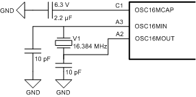
The TPS659038-Q1 and TPS659039-Q1 have the ability to accept a 16-MHz crystal input. Providing the 16-MHz crystal input to the device allows the output of a stable and accurate 32-kHz clock to be used by the applications processor. The crystal input is divided down by 500 internally to produce the 32-kHz output clock. The crystal should be connected to the device as shown in Figure 7-6.
 Figure 7-6 Crystal Input Configuration
 As shown in Figure 7-6, the OSC16MCAP pin requires a 2.2-µF 6.3-V filtering capacitor near the ball. Also, the crystal requires between 9 pF and 11 pF of load capacitance on both terminals. To meet this requirement, using two 10-pF capacitors is recommended. See Table 7-2 for the specific load capacitors that are recommended.
The 16-MHz crystal is not required for operation of the TPS659038-Q1 and TPS659039-Q1 devices. The OSC16M_CFG OTP bit can be set to disable the 16-MHz crystal completely, and enable the following 2 alternative options for system clock generation:
- A 32-kHz square wave can be supplied to the OSC16MIN pin. This option is typically used in applications where the processor requires an accurate system clock and there is one already available in the system. In that case, the available 32-kHz clock can be provided to the PMIC and added to the boot sequence as an output. In this configuration, the OSC16MOUT and OSC16MCAP pins can be left floating, and the internal 16-MHz oscillator is bypassed. Bypassing the 16-MHz oscillator results in a lower quiescent current.
- If the application does not require an accurate system clock for the processor, then providing one to the PMIC is not required. This option produces a lower quiescent current as seen in Section 5. In this configuration, the OSC16MIN pin should be grounded, while the OSC16MOUT and OSCMCAP pins can be left floating. Lastly, the GATE_RESET_OUT OTP bit should be used to allow the device to power up without the presence of the 16.384-MHz crystal nor the 32-kHz clock input.
If the OSC16M_CFG OTP bit is set to 0, a 16-MHz crystal must be present for the proper operation of the device.