SBVS054K November 2004 – June 2025 TPS730
PRODUCTION DATA
- 1
- 1 Features
- 2 Applications
- 3 Description
- 4 Pin Configuration and Functions
- 5 Specifications
- 6 Detailed Description
- 7 Application and Implementation
- 8 Device and Documentation Support
- 9 Revision History
- 10Mechanical, Packaging, and Orderable Information
Package Options
Mechanical Data (Package|Pins)
Thermal pad, mechanical data (Package|Pins)
Orderable Information
7.5.1.3 Power Dissipation
Specified regulator operation is assured to a junction temperature of +125°C; the maximum junction temperature should be restricted to +125°C under normal operating conditions. This restriction limits the power dissipation the regulator can handle in any given application. To ensure the junction temperature is within acceptable limits, calculate the maximum allowable dissipation, PD(max), and the actual dissipation, PD, which must be less than or equal to PD(max).
The maximum power dissipation limit is determined using Equation 4:

where:
- TJmax is the maximum allowable junction temperature
- RθJA is the thermal resistance junction-to-ambient for the package (see the Thermal Information table)
- TA is the ambient temperature
The regulator dissipation is calculated using Equation 5:

Power dissipation resulting from quiescent current is negligible. Excessive power dissipation triggers the thermal protection circuit.
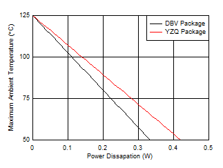
Figure 7-7 illustrates the maximum ambient temperature versus the power dissipation of the TPS730. This figure assumes the device is soldered on a JEDEC standard, high-K layout with no airflow over the board. Actual board thermal impedances vary widely. If the application requires high power dissipation, having a thorough understanding of the board temperature and thermal impedances is helpful to ensure the TPS730 does not operate above a junction temperature of 125°C.
 Figure 7-7 Maximum Ambient Temperature vs Power Dissipation
Estimating the junction temperature can be done by using the thermal metrics ΨJT and ΨJB, shown in the Thermal Information table. These metrics are a more accurate representation of the heat transfer characteristics of the die and the package than RθJA. The junction temperature can be estimated with Equation 6.

where:
- PD is the power dissipation shown by Equation 5
- TT is the temperature at the center-top of the device package
- TB is the PCB temperature measured 1 mm away from the device package on the PCB surface
Both TT and TB can be measured on actual application boards using a thermo‐gun (an infrared thermometer).
For more information about measuring TT and TB, see the Using New Thermal Metrics application note, available for download at www.ti.com.