SLVSER5A December 2018 – May 2021 TPS73801-SEP
PRODUCTION DATA
- 1 Features
- 2 Applications
- 3 Description
- 4 Revision History
- 5 Pin Configuration and Functions
- 6 Specifications
- 7 Detailed Description
- 8 Application and Implementation
- 9 Power Supply Recommendations
- 10Layout
- 11Device and Documentation Support
- 12Mechanical, Packaging, and Orderable Information
Package Options
Mechanical Data (Package|Pins)
- DCQ|6
Thermal pad, mechanical data (Package|Pins)
Orderable Information
8.2.2 Detailed Design Procedure
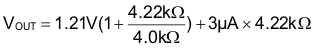
The TPS73801-SEP has an adjustable output voltage range of 1.21 to 20 V. The output voltage is set by the ratio of two external resistors R1 and R2 as shown in Figure 8-1. The device maintains the voltage at the FB pin at 1.21 V referenced to ground. The current in R1 is then equal to (1.21 V / R1), and the current in R2 is the current in R1 plus the FB pin bias current. The FB pin bias current, 3 µA at 25°C, flows through R2 into the FB pin. The output voltage can be calculated using Equation 5.
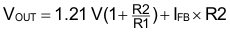
The value of R1 should be less than 4.17 kΩ to minimize errors in the output voltage caused by the FB pin bias current. Note that in shutdown the output is turned off, and the divider current is zero. For an output voltage of 2.50 V, R1 will be set to 4.0 kΩ. R2 is then found to be 4.22 kΩ using the equation above.
The adjustable device is tested and specified with the FB pin tied to the OUT pin for an output voltage of 1.21 V. Specifications for output voltages greater than 1.21 V are proportional to the ratio of the desired output voltage to 1.21 V: VOUT / 1.21 V. For example, load regulation for an output current change of 1 mA to 1.5 A is –2 mV (typ) at VOUT = 1.21 V. At VOUT = 2.50 V, the typical load regulation is:
Figure 8-2 shows the actual change in output is approximately 3 mV for a 1-A load step. The maximum load regulation at 25°C is –8 mV. At VOUT = 2.50 V, the maximum load regulation is:
Since 16.53 mV is 0.7% of the 2.5-V output voltage, the load regulation will meet the design requirements.