SBVS065L December 2005 – December 2024 TPS74301
PRODUCTION DATA
- 1
- 1 Features
- 2 Applications
- 3 Description
- 4 Pin Configurations and Functions
- 5 Specifications
- 6 Detailed Description
- 7 Application and Implementation
- 8 Device and Documentation Support
- 9 Revision History
- 10Mechanical, Packaging, and Orderable Information
Package Options
Mechanical Data (Package|Pins)
Thermal pad, mechanical data (Package|Pins)
- RGW|20
Orderable Information
7.4.1.1 Layout Recommendations and Power Dissipation
An optimal layout can greatly improve transient performance, PSRR, and noise. To minimize the voltage droop on the input of the device during load transients, the capacitance on IN and BIAS must be connected as close as possible to the device. This capacitance also minimizes the effects of parasitic inductance and resistance of the input source and can therefore improve stability. To achieve optimal transient performance and accuracy, the top side of R1 in Figure 7-4 must be connected as close as possible to the load. If BIAS is connected to IN, connecting the BIAS as close as possible to the sense point of the input supply is recommended. This connection minimizes the voltage droop on BIAS during transient conditions and can improve the turn-on response.
Knowing the device power dissipation and proper sizing of the thermal plane that is connected to the tab or pad is critical to avoiding thermal shutdown and providing reliable operation. Power dissipation of the device depends on input voltage and load conditions, and can be calculated using Equation 1:

Power dissipation can be minimized and greater efficiency can be achieved by using the lowest possible input voltage necessary to achieve the required output voltage regulation.
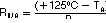
On the QFN (RGW) package, the primary conduction path for heat is through the exposed pad to the printed circuit board (PCB). The pad can be connected to ground or be left floating; however, the pad must be attached to an appropriate amount of copper PCB area to verify the device does not overheat. On the DDPAK (KTW) package, the primary conduction path for heat is through the tab to the PCB. That tab must be connected to ground. The maximum junction-to-ambient thermal resistance depends on the maximum ambient temperature, maximum device junction temperature, and power dissipation of the device and can be calculated using Equation 2:
Knowing the maximum RθJA, the minimum amount of PCB copper area needed for appropriate heatsinking can be estimated using Figure 7-9.

Figure 7-9 shows the variation of θJA as a function of ground plane copper area in the board. This figure is intended only as a guideline to demonstrate the effects of heat spreading in the ground plane and must not be used to estimate actual thermal performance in real application environments.