SGLS247C September 2011 – December 2025 TPS763-Q1
PRODUCTION DATA
- 1
- 1 Features
- 2 Applications
- 3 Description
- 4 Pin Configuration and Functions
- 5 Specifications
- 6 Detailed Description
-
7 Application and Implementation
- 7.1 Application Information
- 7.2 Typical Application
- 7.3 Power Supply Recommendations
- 7.4 Layout
- 8 Device and Documentation Support
- 9 Revision History
- 10Mechanical, Packaging, and Orderable Information
Package Options
Refer to the PDF data sheet for device specific package drawings
Mechanical Data (Package|Pins)
- DBV|5
Thermal pad, mechanical data (Package|Pins)
Orderable Information
6.3.3 Current Limit
For the legacy chip, the internal current limit circuit protects the LDO against high-load current faults or shorting events. The LDO is not designed to operate in a steady-state current limit. During a current-limit event, the LDO sources constant current. Therefore, the output voltage falls when load impedance decreases. If a current limit occurs and the resulting output voltage is low, excessive power is potentially dissipated across the LDO, resulting in a thermal shutdown of the output. A foldback feature limits the short-circuit current to protect the regulator from damage under all load conditions. If VOUT is forced below 0V before EN goes high and the load current required exceeds the foldback current limit, the device potentially does not start up correctly.
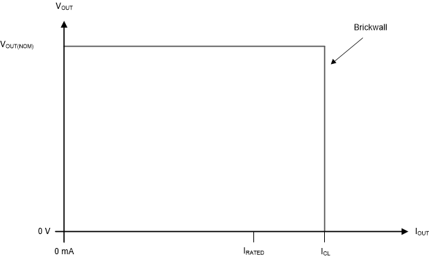
For the new chip, the device has an internal current limit circuit that protects the regulator during transient high-load current faults or shorting events. The current limit is a brick-wall scheme. In a high-load current fault, the brick-wall scheme limits the output current to the current limit (ICL). ICL is listed in the Electrical Characteristics table.
The output voltage is not regulated when the device is in current limit. When a current limit event occurs, the device begins to heat up because of the increase in power dissipation. When the device is in brick-wall current limit, the pass transistor dissipates power [(VIN – VOUT) × ICL]. If thermal shutdown is triggered, the device turns off. After the device cools down, the internal thermal shutdown circuit turns the device back on. If the output current fault condition continues, the device cycles between current limit and thermal shutdown. For more information on current limits, see the Know Your Limits application note.
Figure 6-4 shows a diagram of the current limit.
 Figure 6-4 Current
Limit