SGLS247C September   2011  – December 2025 TPS763-Q1

PRODUCTION DATA  

  1.   1
  2. Features
  3. Applications
  4. Description
  5. Pin Configuration and Functions
  6. Specifications
    1. 5.1 Absolute Maximum Ratings
    2. 5.2 ESD Ratings
    3. 5.3 Recommended Operating Conditions
    4. 5.4 Thermal Information
    5. 5.5 Electrical Characteristics
    6. 5.6 Typical Characteristics
  7. Detailed Description
    1. 6.1 Overview
    2. 6.2 Functional Block Diagram
    3. 6.3 Feature Description
      1. 6.3.1 Output Enable
      2. 6.3.2 Dropout Voltage
      3. 6.3.3 Current Limit
      4. 6.3.4 Output Pulldown
      5. 6.3.5 Thermal Shutdown
    4. 6.4 Device Functional Modes
      1. 6.4.1 Device Functional Mode Comparison
      2. 6.4.2 Normal Operation
      3. 6.4.3 Dropout Operation
      4. 6.4.4 Disabled
  8. Application and Implementation
    1. 7.1 Application Information
      1. 7.1.1 Adjustable Device Feedback Resistors
      2. 7.1.2 Recommended Capacitor Types
        1. 7.1.2.1 Recommended Capacitors (Legacy Chip)
        2. 7.1.2.2 Recommended Capacitors (New Chip)
      3. 7.1.3 Input and Output Capacitor Requirements
        1. 7.1.3.1 Input Capacitor Requirements
        2. 7.1.3.2 Output Capacitor Requirements
      4. 7.1.4 Reverse Current
      5. 7.1.5 Feed-Forward Capacitor (CFF)
      6. 7.1.6 Power Dissipation (PD)
      7. 7.1.7 Estimating Junction Temperature
    2. 7.2 Typical Application
      1. 7.2.1 Design Requirements
      2. 7.2.2 Detailed Design Procedure
        1. 7.2.2.1 Output Voltage Programming
      3. 7.2.3 Application Curves
    3. 7.3 Power Supply Recommendations
    4. 7.4 Layout
      1. 7.4.1 Layout Guidelines
      2. 7.4.2 Layout Example
      3. 7.4.3 Power Dissipation and Junction Temperature
  9. Device and Documentation Support
    1. 8.1 Device Support
      1. 8.1.1 Third-Party Products Disclaimer
    2. 8.2 Documentation Support
      1. 8.2.1 Device Nomenclature
      2. 8.2.2 Related Documentation
    3. 8.3 Receiving Notification of Documentation Updates
    4. 8.4 Support Resources
    5. 8.5 Trademarks
    6. 8.6 Electrostatic Discharge Caution
    7. 8.7 Glossary
  10. Revision History
  11. 10Mechanical, Packaging, and Orderable Information

Package Options

Refer to the PDF data sheet for device specific package drawings

Mechanical Data (Package|Pins)
  • DBV|5
Thermal pad, mechanical data (Package|Pins)
Orderable Information

Description

The TPS763xx-Q1 family of low-dropout (LDO) linear voltage regulators supports wide input voltage range of 2.7V to 10V and up-to 150mA of load current. The output range is from 1.6V to 5.0V for fixed version, and 1.6V to 6.5V for adjustable version.

The TPS763xx-Q1 has a ±1.5% output accuracy that is required for powering digital loads with tight supply requirements. The internal soft-start circuit reduces inrush current during start-up (for new chip), thus allowing for smaller input capacitance.

The TPS763xx-Q1 family of low-dropout (LDO) voltage regulators offers the benefits of low-dropout voltage, low-power operation, and miniaturized packaging. These regulators feature low dropout voltages and quiescent currents compared to conventional LDO regulators. Offered in a 5-pin, small outline integrated-circuit SOT-23 package, the TPS763xx-Q1 series devices are and excellent choice for cost-sensitive designs and applications where board space is at a premium.

The TPS763xx-Q1 also features a logic-enabled sleep mode to shut down the regulator, reducing quiescent current to 1μA maximum at TJ = 25°C.
Package Information
PART NUMBER PACKAGE(1) PACKAGE SIZE (2)
TPS763xx-Q1 SOT-23 (5) 2.9mm × 2.8mm
For all available packages, see the orderable addendum at the end of the data sheet.
The package size (length × width) is a nominal value and includes pins, where applicable.
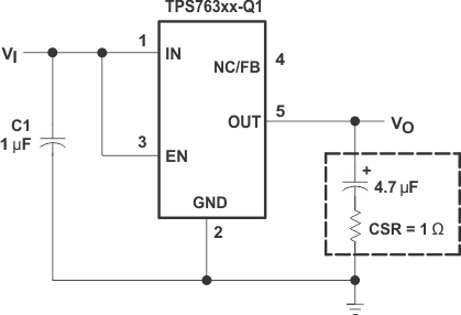
TPS763-Q1 Typical Application Circuit Typical Application Circuit