SGLS247C September   2011  – December 2025 TPS763-Q1

PRODUCTION DATA  

  1.   1
  2. Features
  3. Applications
  4. Description
  5. Pin Configuration and Functions
  6. Specifications
    1. 5.1 Absolute Maximum Ratings
    2. 5.2 ESD Ratings
    3. 5.3 Recommended Operating Conditions
    4. 5.4 Thermal Information
    5. 5.5 Electrical Characteristics
    6. 5.6 Typical Characteristics
  7. Detailed Description
    1. 6.1 Overview
    2. 6.2 Functional Block Diagram
    3. 6.3 Feature Description
      1. 6.3.1 Output Enable
      2. 6.3.2 Dropout Voltage
      3. 6.3.3 Current Limit
      4. 6.3.4 Output Pulldown
      5. 6.3.5 Thermal Shutdown
    4. 6.4 Device Functional Modes
      1. 6.4.1 Device Functional Mode Comparison
      2. 6.4.2 Normal Operation
      3. 6.4.3 Dropout Operation
      4. 6.4.4 Disabled
  8. Application and Implementation
    1. 7.1 Application Information
      1. 7.1.1 Adjustable Device Feedback Resistors
      2. 7.1.2 Recommended Capacitor Types
        1. 7.1.2.1 Recommended Capacitors (Legacy Chip)
        2. 7.1.2.2 Recommended Capacitors (New Chip)
      3. 7.1.3 Input and Output Capacitor Requirements
        1. 7.1.3.1 Input Capacitor Requirements
        2. 7.1.3.2 Output Capacitor Requirements
      4. 7.1.4 Reverse Current
      5. 7.1.5 Feed-Forward Capacitor (CFF)
      6. 7.1.6 Power Dissipation (PD)
      7. 7.1.7 Estimating Junction Temperature
    2. 7.2 Typical Application
      1. 7.2.1 Design Requirements
      2. 7.2.2 Detailed Design Procedure
        1. 7.2.2.1 Output Voltage Programming
      3. 7.2.3 Application Curves
    3. 7.3 Power Supply Recommendations
    4. 7.4 Layout
      1. 7.4.1 Layout Guidelines
      2. 7.4.2 Layout Example
      3. 7.4.3 Power Dissipation and Junction Temperature
  9. Device and Documentation Support
    1. 8.1 Device Support
      1. 8.1.1 Third-Party Products Disclaimer
    2. 8.2 Documentation Support
      1. 8.2.1 Device Nomenclature
      2. 8.2.2 Related Documentation
    3. 8.3 Receiving Notification of Documentation Updates
    4. 8.4 Support Resources
    5. 8.5 Trademarks
    6. 8.6 Electrostatic Discharge Caution
    7. 8.7 Glossary
  10. Revision History
  11. 10Mechanical, Packaging, and Orderable Information

Package Options

Refer to the PDF data sheet for device specific package drawings

Mechanical Data (Package|Pins)
  • DBV|5
Thermal pad, mechanical data (Package|Pins)
Orderable Information

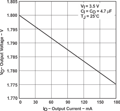
Typical Characteristics

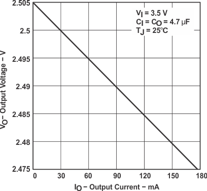
TPS763-Q1 TPS76325-Q1 Output
            Voltage vs Output Current (Legacy Chip)
Figure 5-1 TPS76325-Q1 Output Voltage vs Output Current (Legacy Chip)
TPS763-Q1 TPS76333-Q1
            Output Voltage vs Output Current (new chip)
Figure 5-3 TPS76333-Q1 Output Voltage vs Output Current (new chip)
TPS763-Q1 TPS76333-Q1 Output Voltage vs Output Current (new
            chip)
Figure 5-5 TPS76333-Q1 Output Voltage vs Output Current (new chip)
TPS763-Q1 TPS76333-Q1 Short-circuit current vs Output voltage (new
            chip)
Figure 5-7 TPS76333-Q1 Short-circuit current vs Output voltage (new chip)
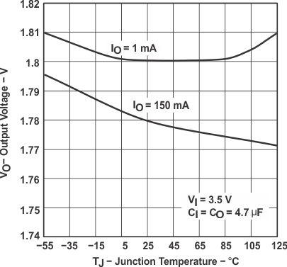
TPS763-Q1 TPS76318-Q1 Output
            Voltage vs Free-Air Temperature (Legacy Chip)
Figure 5-9 TPS76318-Q1 Output Voltage vs Free-Air Temperature (Legacy Chip)
TPS763-Q1 TPS76350-Q1 Ground
            Current vs Free-Air Temperature (Legacy Chip)
Figure 5-11 TPS76350-Q1 Ground Current vs Free-Air Temperature (Legacy Chip)
TPS763-Q1 Input Current vs Input Voltage  (new
            chip)
 
Figure 5-13 Input Current vs Input Voltage (new chip)
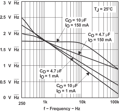
TPS763-Q1 Output Noise vs Frequency
            (Legacy Chip)
Figure 5-15 Output Noise vs Frequency (Legacy Chip)
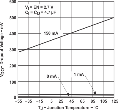
TPS763-Q1 TPS76325-Q1 Dropout
            Voltage vs Free-Air Temperature (Legacy Chip)
Figure 5-17 TPS76325-Q1 Dropout Voltage vs Free-Air Temperature (Legacy Chip)
TPS763-Q1 TPS76333-Q1 Dropout Voltage vs Load
            Current (new chip)
 
Figure 5-19 TPS76333-Q1 Dropout Voltage vs Load Current (new chip)
TPS763-Q1 TPS76318-Q1 Line
            Transient Response (Legacy Chip)
Figure 5-21 TPS76318-Q1 Line Transient Response (Legacy Chip)
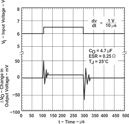
TPS763-Q1 TPS76350-Q1 Line
            Transient Response (Legacy Chip)
Figure 5-23 TPS76350-Q1 Line Transient Response (Legacy Chip)
TPS763-Q1 Line Transient
            Response (New Chip)
VOUT = 3.3V, IL = 100mA
Figure 5-25 Line Transient Response (New Chip)
TPS763-Q1 Load Transient
            Response (New Chip)
VOUT = 3.3V, COUT = 2.2μF
Figure 5-27 Load Transient Response (New Chip)
TPS763-Q1 Ripple
            Rejection versus Output Capacitor (CL) and Frequency (New Chip)
Figure 5-29 Ripple Rejection versus Output Capacitor (CL) and Frequency (New Chip)
TPS763-Q1 Turn-on
            Waveform (New Chip)
VOUT = 3.3V, RL = 3.3kΩ
Figure 5-31 Turn-on Waveform (New Chip)
TPS763-Q1 Short Circuit
            Current versus Time (New Chip)
VIN = 4.3V
Figure 5-33 Short Circuit Current versus Time (New Chip)
TPS763-Q1 Typical Regions of
            Stability Compensation Series Resistance (CSR) vs Output Current (Legacy Chip)
Figure 5-35 Typical Regions of Stability Compensation Series Resistance (CSR) vs Output Current (Legacy Chip)
TPS763-Q1 Typical Regions of
            Stability Compensation Series Resistance (CSR) vs Output Current (Legacy Chip)
Figure 5-37 Typical Regions of Stability Compensation Series Resistance (CSR) vs Output Current (Legacy Chip)
TPS763-Q1 TPS76318-Q1 Output
            Voltage vs Output Current (Legacy Chip)
Figure 5-2 TPS76318-Q1 Output Voltage vs Output Current (Legacy Chip)
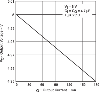
TPS763-Q1 TPS76350-Q1
            Output Voltage vs Output Current (Legacy Chip)
Figure 5-4 TPS76350-Q1 Output Voltage vs Output Current (Legacy Chip)
TPS763-Q1 TPS76333-Q1 Output Voltage vs Input Voltage (new chip)
Figure 5-6 TPS76333-Q1 Output Voltage vs Input Voltage (new chip)
TPS763-Q1 TPS76325-Q1 Output
            Voltage vs Free-Air Temperature (Legacy Chip)
Figure 5-8 TPS76325-Q1 Output Voltage vs Free-Air Temperature (Legacy Chip)
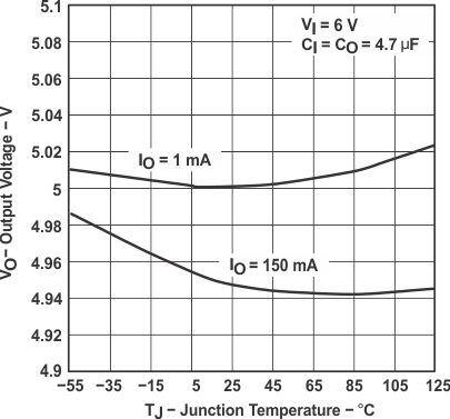
TPS763-Q1 TPS76350-Q1 Output
            Voltage vs Free-Air Temperature (Legacy Chip)
Figure 5-10 TPS76350-Q1 Output Voltage vs Free-Air Temperature (Legacy Chip)
TPS763-Q1 Ground Pin Current vs Load Current
            (new chip)
 
Figure 5-12 Ground Pin Current vs Load Current (new chip)
TPS763-Q1 Ground-Pin
            Current vs Temperature  (new chip)
 
Figure 5-14 Ground-Pin Current vs Temperature (new chip)
TPS763-Q1 Output Impedance vs
            Frequency (Legacy Chip)
Figure 5-16 Output Impedance vs Frequency (Legacy Chip)
TPS763-Q1 TPS76333-Q1 Dropout Voltage vs
            Temperature (new chip)
 
Figure 5-18 TPS76333-Q1 Dropout Voltage vs Temperature (new chip)
TPS763-Q1 TPS76325-Q1 Ripple
            Rejection vs Frequency (Legacy Chip)
Figure 5-20 TPS76325-Q1 Ripple Rejection vs Frequency (Legacy Chip)
TPS763-Q1 TPS76318-Q1 Load
            Transient Response (Legacy Chip)
Figure 5-22 TPS76318-Q1 Load Transient Response (Legacy Chip)
TPS763-Q1 TPS76350-Q1 Load
            Transient Response (Legacy Chip)
Figure 5-24 TPS76350-Q1 Load Transient Response (Legacy Chip)
TPS763-Q1 Line Transient
            Response (New Chip)
VOUT = 3.3V, IL = 1mA
Figure 5-26 Line Transient Response (New Chip)
TPS763-Q1 Ripple
            Rejection versus Load Current (IL) and Frequency (New Chip)
Figure 5-28 Ripple Rejection versus Load Current (IL) and Frequency (New Chip)
TPS763-Q1 Output Noise
            Density versus Load Current (IL) Frequency (New Chip)
Figure 5-30 Output Noise Density versus Load Current (IL) Frequency (New Chip)
TPS763-Q1 Turn-off
            Waveform (New Chip)
VOUT = 5V, RL = 5kΩ
Figure 5-32 Turn-off Waveform (New Chip)
TPS763-Q1 Short Circuit
            Current versus Time (New Chip)
VIN = 10.0V
Figure 5-34 Short Circuit Current versus Time (New Chip)
TPS763-Q1 Typical Regions of
            Stability Compensation Series Resistance (CSR) vs Added Ceramic Capacitance (Legacy
            Chip)
Figure 5-36 Typical Regions of Stability Compensation Series Resistance (CSR) vs Added Ceramic Capacitance (Legacy Chip)
TPS763-Q1 Typical Regions of
            Stability Compensation Series Resistance (CSR) vs Added Ceramic (Legacy Chip)
Figure 5-38 Typical Regions of Stability Compensation Series Resistance (CSR) vs Added Ceramic (Legacy Chip)