SBVS115D August 2008 – January 2015 TPS782
PRODUCTION DATA.
- 1 Features
- 2 Applications
- 3 Description
- 4 Revision History
- 5 Pin Configuration and Functions
- 6 Specifications
- 7 Detailed Description
- 8 Application and Implementation
- 9 Power Supply Recommendations
- 10Layout
- 11Device and Documentation Support
- 12Mechanical, Packaging, and Orderable Information
Package Options
Mechanical Data (Package|Pins)
Thermal pad, mechanical data (Package|Pins)
- DRV|6
Orderable Information
8 Application and Implementation
NOTE
Information in the following applications sections is not part of the TI component specification, and TI does not warrant its accuracy or completeness. TI’s customers are responsible for determining suitability of components for their purposes. Customers should validate and test their design implementation to confirm system functionality.
8.1 Application Information
The TPS782 family of LDOs is factory-programmable to have a fixed output. Note that during startup or steady-state conditions, it is important that the EN pin voltage never exceed VIN + 0.3V.
8.2 Typical Application
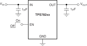 Figure 23. Typical Application Circuit
8.2.1 Design Requirements
Select the desired device based on the output voltage.
Provide an input supply with adequate headroom to account for dropout and output current to account for the GND pin current, and power the load. Select input and output capacitors based on application needs.
8.2.2 Detailed Design Procedure
8.2.2.1 Input and Output Capacitor Requirements
Although an input capacitor is not required for stability, it is good analog design practice to connect a 0.1-μF to 1.0-μF low equivalent series resistance (ESR) capacitor across the input supply near the regulator. This capacitor counteracts reactive input sources and improves transient response, noise rejection, and ripple rejection. A higher-value capacitor may be necessary if large, fast rise-time load transients are anticipated, or if the device is not located near the power source. If source impedance is not sufficiently low, a 0.1-μF input capacitor may be necessary to ensure stability.
The TPS782 series is designed to be stable with standard ceramic capacitors with values of 1.0 μF or larger at the output. X5R- and X7R-type capacitors are best because they have minimal variation in value and ESR over temperature. Maximum ESR should be less than 1.0 Ω. With tolerance and dc bias effects, the minimum capacitance to ensure stability is 1 μF.
8.2.2.2 Dropout Voltage
The TPS782 uses a PMOS pass transistor to achieve low dropout. When (VIN – VOUT) is less than the dropout voltage (VDO), the PMOS pass device is the linear region of operation and the input-to-output resistance is the RDS(ON) of the PMOS pass element. VDO approximately scales with output current because the PMOS device behaves like a resistor in dropout. As with any linear regulator, PSRR and transient response are degraded as (VIN – VOUT) approaches dropout. This effect is shown in the Typical Characteristics section. Refer to application report SLVA207,Understanding LDO Dropout, available for download from www.ti.com.
8.2.2.3 Transient Response
As with any regulator, increasing the size of the output capacitor reduces over/undershoot magnitude but increases duration of the transient response. For more information, see Figure 19.
8.2.2.4 Minimum Load
The TPS782 series is stable with no output load. Traditional PMOS LDO regulators suffer from lower loop gain at very light output loads. The TPS782 employs an innovative, low-current circuit under very light or no-load conditions, resulting in improved output voltage regulation performance down to zero output current. See Figure 19 for the load transient response.
8.2.3 Application Curves
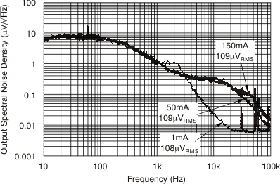 Figure 24. Output Spectral Noise Density vs Frequency, CIN = 1 μF, COUT = 2.2 μF, VIN = 3.2 V, TPS78227
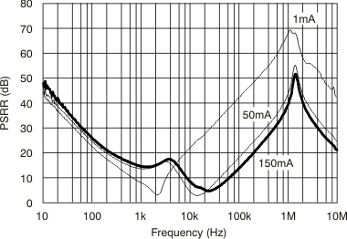 Figure 25. Ripple Rejection vs Frequency, VIN = 4.2 V,
 VOUT = 2.7 V, COUT = 2.2 μF, TPS78227
8.3 Do's and Don’ts
Do place at least one 1-µF ceramic capacitor as close as possible to the OUT pin of the regulator.
Do not place the output capacitor more than 10 mm away from the regulator.
Do connect a 0.1-μF to 1.0-μF low equivalent series resistance (ESR) capacitor across the IN pin and GND of the regulator.
Do not exceed the absolute maximum ratings.