SBVS115D August 2008 – January 2015 TPS782
PRODUCTION DATA.
- 1 Features
- 2 Applications
- 3 Description
- 4 Revision History
- 5 Pin Configuration and Functions
- 6 Specifications
- 7 Detailed Description
- 8 Application and Implementation
- 9 Power Supply Recommendations
- 10Layout
- 11Device and Documentation Support
- 12Mechanical, Packaging, and Orderable Information
Package Options
Mechanical Data (Package|Pins)
Thermal pad, mechanical data (Package|Pins)
- DRV|6
Orderable Information
7 Detailed Description
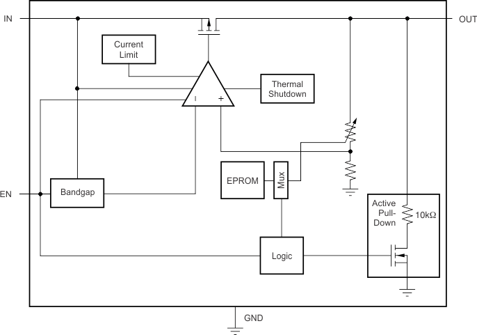
7.1 Overview
The TPS782 family of low-dropout regulators (LDOs) is designed specifically for battery-powered applications where ultralow quiescent current is a critical parameter. The TPS782 family is compatible with the TI MSP430 and other similar products. The enable pin (EN) is compatible with standard CMOS logic. This LDO family is stable with any output capacitor greater than 1.0 µF.
7.2 Functional Block Diagram
7.3 Feature Description
7.3.1 Internal Current Limit
The TPS782 is internally current-limited to protect the regulator during fault conditions. During current limit, the output sources a fixed amount of current that is largely independent of output voltage. For reliable operation, the device should not be operated in a current limit state for extended periods of time.
The PMOS pass element in the TPS782 series has a built-in body diode that conducts current when the voltage at OUT exceeds the voltage at IN. This current is not limited, so if extended reverse voltage operation is anticipated, external limiting to 5% of rated output current may be appropriate.
7.3.2 Active VOUT Pulldown
In the TPS782 series, the active pulldown discharges VOUT when the device is off. However, the input voltage must be greater than 2.2 V for the active pulldown to work.
7.3.3 Shutdown
The enable pin (EN) is active high and is compatible with standard and low-voltage CMOS levels. When shutdown capability is not required, EN should be connected to the IN pin, as shown in Figure 22. The TPS782 series, with internal active output pulldown circuitry, discharges the output to within 5% VOUT with a time (t) shown in Equation 1:
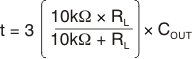
Where:
RL= output load resistance
COUT = output capacitance
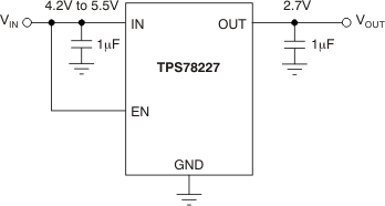 Figure 22. Circuit Showing EN Tied High When Shutdown Capability Is Not Required
7.4 Device Functional Modes
Table 1 provides a quick comparison between the normal, dropout, and disabled modes of operation.
Table 1. Device Functional Mode Comparison
| OPERATING MODE | PARAMETER | |||
|---|---|---|---|---|
| VIN | EN | IOUT | TJ | |
| Normal | VIN > VOUT(nom) + VDO | VEN > VEN(HI) | IOUT < ILIM | TJ < TSD |
| Dropout | VIN < VOUT(nom) + VDO | VEN > VEN(HI) | IOUT < ILIM | TJ < TSD |
| Disabled | — | VEN < VEN(LO) | — | TJ > TSD |
7.4.1 Normal Operation
The device regulates to the nominal output voltage under the following conditions:
- The input voltage is greater than the nominal output voltage plus the dropout voltage (VOUT(nom) + VDO).
- The enable voltage has previously exceeded the enable rising threshold voltage and not yet decreased below the enable falling threshold.
- The output current is less than the current limit (IOUT < ILIM).
- The device junction temperature is less than the thermal shutdown temperature (TJ < TSD).
7.4.2 Dropout Operation
If the input voltage is lower than the nominal output voltage plus the specified dropout voltage, but all other conditions are met for normal operation, the device operates in dropout mode. In this mode, the output voltage tracks the input voltage. During this mode, the transient performance of the device becomes significantly degraded because the pass device is in a triode state and no longer controls the current through the LDO. Line or load transients in dropout can result in large output-voltage deviations.
7.4.3 Disabled
The device is disabled under the following conditions:
- The enable voltage is less than the enable falling threshold voltage or has not yet exceeded the enable rising threshold.
- The device junction temperature is greater than the thermal shutdown temperature (TJ > TSD).