SBVS388B January   2021  – January 2022 TPS785-Q1

PRODUCTION DATA  

  1. Features
  2. Applications
  3. Description
  4. Revision History
  5. Pin Configuration and Functions
  6. Specifications
    1. 6.1 Absolute Maximum Ratings
    2. 6.2 ESD Ratings
    3. 6.3 Recommended Operating Conditions
    4. 6.4 Thermal Information
    5. 6.5 Electrical Characteristics
    6. 6.6 Typical Characteristics
  7. Detailed Description
    1. 7.1 Overview
    2. 7.2 Functional Block Diagrams
    3. 7.3 Feature Description
      1. 7.3.1 Foldback Current Limit
      2. 7.3.2 Output Enable
      3. 7.3.3 Active Discharge
      4. 7.3.4 Undervoltage Lockout (UVLO) Operation
      5. 7.3.5 Dropout Voltage
      6. 7.3.6 Thermal Shutdown
    4. 7.4 Device Functional Modes
      1. 7.4.1 Device Functional Mode Comparison
      2. 7.4.2 Normal Operation
      3. 7.4.3 Dropout Operation
      4. 7.4.4 Disabled
  8. Application and Implementation
    1. 8.1 Application Information
      1. 8.1.1 Recommended Capacitor Types
      2. 8.1.2 Input and Output Capacitor Requirements
      3. 8.1.3 Adjustable Device Feedback Resistors
      4. 8.1.4 Load Transient Response
      5. 8.1.5 Exiting Dropout
      6. 8.1.6 Dropout Voltage
      7. 8.1.7 Reverse Current
      8. 8.1.8 Feed-Forward Capacitor (CFF)
      9. 8.1.9 Power Dissipation (PD)
        1. 8.1.9.1 Estimating Junction Temperature
        2. 8.1.9.2 Recommended Area for Continuous Operation
        3. 8.1.9.3 Power Dissipation versus Ambient Temperature
    2. 8.2 Typical Application
      1. 8.2.1 Design Requirements
      2. 8.2.2 Detailed Design Procedure
      3. 8.2.3 Application Curve
  9. Power Supply Recommendations
  10. 10Layout
    1. 10.1 Layout Guidelines
      1. 10.1.1 Additional Layout Considerations
    2. 10.2 Layout Examples
  11. 11Device and Documentation Support
    1. 11.1 Device Support
      1. 11.1.1 Device Nomenclature
    2. 11.2 Documentation Support
      1. 11.2.1 Related Documentation
    3. 11.3 Receiving Notification of Documentation Updates
    4. 11.4 Support Resources
    5. 11.5 Trademarks
    6. 11.6 Electrostatic Discharge Caution
    7. 11.7 Glossary
  12. 12Mechanical, Packaging, and Orderable Information

Package Options

Mechanical Data (Package|Pins)
Thermal pad, mechanical data (Package|Pins)
Orderable Information

Power Dissipation versus Ambient Temperature

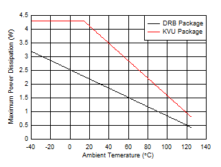
Figure 8-7 is based off of a JESD51-7 four-layer high-K board. The allowable power dissipation was estimated using the following equation. As disscussed in the An empirical analysis of the impact of board layout on LDO thermal performance application report, thermal dissipation can be improved in the JEDEC high-K layout by adding top layer copper and increasing the number of thermal vias. If a good thermal layout is used, the allowable thermal dissipation can be improved by up to 50%.
Equation 8. TA + RθJA x PD ≤ 150°C
GUID-B910FA7A-D20B-4B7D-BFBC-78D5845EA914-low.gif Figure 8-7 Allowable Power Dissipation