SBVS388B January   2021  – January 2022 TPS785-Q1

PRODUCTION DATA  

  1. Features
  2. Applications
  3. Description
  4. Revision History
  5. Pin Configuration and Functions
  6. Specifications
    1. 6.1 Absolute Maximum Ratings
    2. 6.2 ESD Ratings
    3. 6.3 Recommended Operating Conditions
    4. 6.4 Thermal Information
    5. 6.5 Electrical Characteristics
    6. 6.6 Typical Characteristics
  7. Detailed Description
    1. 7.1 Overview
    2. 7.2 Functional Block Diagrams
    3. 7.3 Feature Description
      1. 7.3.1 Foldback Current Limit
      2. 7.3.2 Output Enable
      3. 7.3.3 Active Discharge
      4. 7.3.4 Undervoltage Lockout (UVLO) Operation
      5. 7.3.5 Dropout Voltage
      6. 7.3.6 Thermal Shutdown
    4. 7.4 Device Functional Modes
      1. 7.4.1 Device Functional Mode Comparison
      2. 7.4.2 Normal Operation
      3. 7.4.3 Dropout Operation
      4. 7.4.4 Disabled
  8. Application and Implementation
    1. 8.1 Application Information
      1. 8.1.1 Recommended Capacitor Types
      2. 8.1.2 Input and Output Capacitor Requirements
      3. 8.1.3 Adjustable Device Feedback Resistors
      4. 8.1.4 Load Transient Response
      5. 8.1.5 Exiting Dropout
      6. 8.1.6 Dropout Voltage
      7. 8.1.7 Reverse Current
      8. 8.1.8 Feed-Forward Capacitor (CFF)
      9. 8.1.9 Power Dissipation (PD)
        1. 8.1.9.1 Estimating Junction Temperature
        2. 8.1.9.2 Recommended Area for Continuous Operation
        3. 8.1.9.3 Power Dissipation versus Ambient Temperature
    2. 8.2 Typical Application
      1. 8.2.1 Design Requirements
      2. 8.2.2 Detailed Design Procedure
      3. 8.2.3 Application Curve
  9. Power Supply Recommendations
  10. 10Layout
    1. 10.1 Layout Guidelines
      1. 10.1.1 Additional Layout Considerations
    2. 10.2 Layout Examples
  11. 11Device and Documentation Support
    1. 11.1 Device Support
      1. 11.1.1 Device Nomenclature
    2. 11.2 Documentation Support
      1. 11.2.1 Related Documentation
    3. 11.3 Receiving Notification of Documentation Updates
    4. 11.4 Support Resources
    5. 11.5 Trademarks
    6. 11.6 Electrostatic Discharge Caution
    7. 11.7 Glossary
  12. 12Mechanical, Packaging, and Orderable Information

Package Options

Mechanical Data (Package|Pins)
Thermal pad, mechanical data (Package|Pins)
Orderable Information

Typical Characteristics

at operating temperature TJ = 25°C, IOUT = 1 mA, VEN = 1.0 V, CIN = 1.0 µF, COUT = 1.0 µF, and VIN = VOUT(NOM) + 0.75 V or 1.7 V (whichever is greater), unless otherwise noted; typical values are at TJ = 25°C
GUID-5172BB20-7BFE-49BB-82CE-D545067F92F2-low.gif
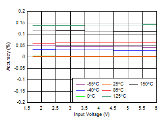
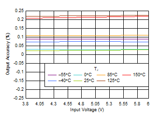
VOUT = 3.3 V
Figure 6-1 Output Accuracy vs VIN
GUID-20210319-CA0I-SGRV-QRTL-WVHDXMZ9SP3V-low.gif
IOUT = 50 mA, VOUT = 1.2 V
Figure 6-3 Output Accuracy vs VIN
GUID-20210317-CA0I-C04S-SVJZ-0S8SGSGCVMXC-low.gif
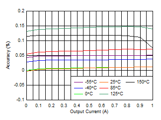
VOUT = 1.2 V
Figure 6-5 Output Accuracy vs Output Current
GUID-20210324-CA0I-GDPM-PQPB-Z1SL3BVFPKBN-low.gif
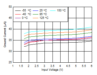
IOUT = 500 µA
Figure 6-7 IGND vs VIN
GUID-20210317-CA0I-JVBN-ZH5H-XKCXWRKZ4LD3-low.gif
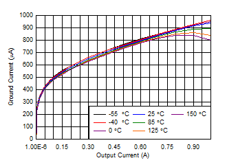
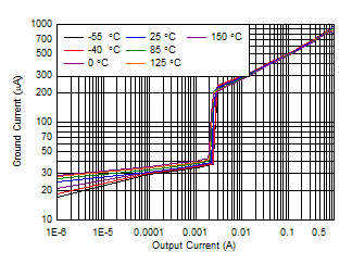
VOUT = 1.2 V, VIN = 2 V
Figure 6-9 IGND vs IOUT
GUID-20210317-CA0I-LCKG-WZ8M-TSDLKXL8DDDX-low.gif
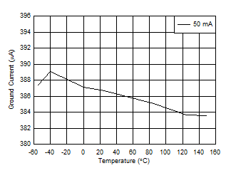
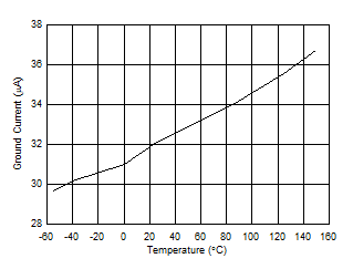
IOUT = 50 mA
Figure 6-11 50-mA Ground Current vs Temperature
GUID-C2BF8265-16EF-4B40-B7C0-E771DF898890-low.gif
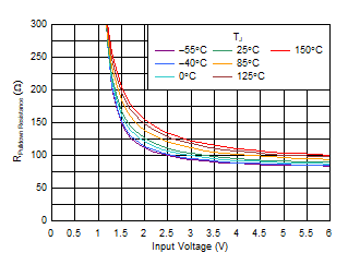
VEN = 0.3 V
Figure 6-13 Pulldown Resistor (RPulldown) vs VIN
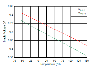
GUID-C3C27628-2C81-40C4-B770-567464192077-low.gif
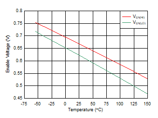
VIN = 6 V
 
Figure 6-15 VEN(HI) and VEN(LOW) Thresholds vs Temperature
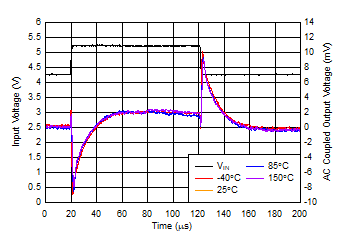
GUID-20210317-CA0I-JDPC-P1ZW-3JRTVFKDMB4J-low.gif
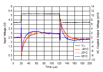
VOUT = 3.3 V, IOUT = 300 mA, slew rate = 1 V/µs
Figure 6-17 Line Transient vs Temperature
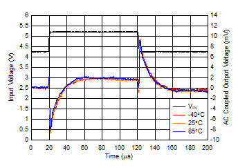
GUID-20210317-CA0I-NHM8-JXSC-4CTDW29GCDCR-low.gif
VOUT = 3.3 V, IOUT = 500 mA, slew rate = 1 V/µs
Figure 6-19 Line Transient vs Temperature
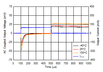
GUID-20210317-CA0I-FKS9-TTFL-67KPJ9JHB1VV-low.gif
VOUT = 3.3 V, IOUT = 0 mA to 100 mA, rise time = 1 µs
Figure 6-21 Load Transient vs Temperature
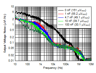
GUID-20210319-CA0I-MG92-BS1H-BTD92KQLZ92Z-low.gif
VOUT = 3.3 V, IOUT = 1 A
Figure 6-23 Noise vs CFF
GUID-20210319-CA0I-CCVG-FM0G-RHQ5PKVCRTGD-low.gif
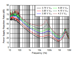
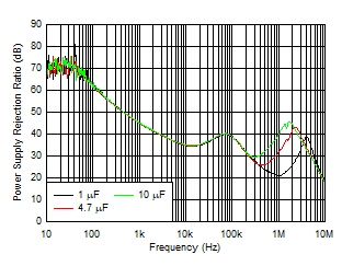
VOUT = 3.3 V, IOUT = 1 A
Figure 6-25 PSRR vs VIN
GUID-20210319-CA0I-TMMF-NN7J-BZHZGCPG1QMC-low.gif
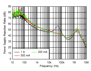
VOUT = 3.3 V
Figure 6-27 PSRR vs IOUT
GUID-DDE1B7E7-D021-4AAA-913E-45DC151B44B8-low.gif
VIN = VEN = 5.5 V, CIN = 0 µF, COUT = 1 µF, VOUT = 1.2 V,
IOUT = 50 mA, TA = -40°C
Figure 6-29 Start Up
GUID-ED732293-FB8A-4BC2-9499-06F6D18F00ED-low.gif
VIN = VEN = 5.5 V, CIN = 0 µF, COUT = 1 µF, VOUT = 1.2 V,
IOUT = 50 mA, TA = 150°C
Figure 6-31 Start Up
GUID-4819613C-B785-4B4D-B9E4-98C38E636AC3-low.gif
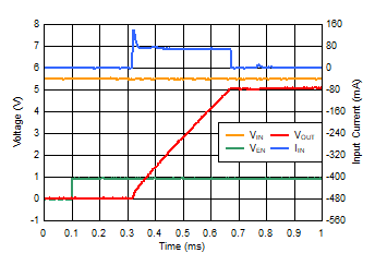
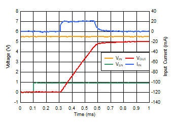
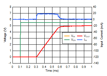
VIN = 5.5 V, CIN = 0 µF, COUT = 4.7 µF, VOUT = 5.0 V,
IOUT = 0 mA
Figure 6-33 Start-Up Inrush Current With
COUT = 4.7 µF
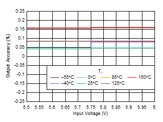
GUID-1B83AA0B-8E73-4E4E-83B4-D2AC26636180-low.gif
VOUT = 5.0 V
Figure 6-2 Output Accuracy vs VIN
GUID-20210317-CA0I-PQVG-ZS4T-BDFL0XPZH3VN-low.gif
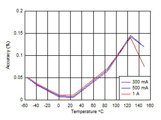
VOUT = 1.2 V
Figure 6-4 Output Accuracy vs Temperature
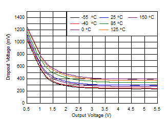
GUID-20210317-CA0I-JJWV-NTVL-2G5MD4DJCFTJ-low.gif
IOUT = 1 A
Figure 6-6 Dropout vs Output Voltage
GUID-20210317-CA0I-VCFH-DSJZ-MF1QFXNHRWQG-low.gif
 
Figure 6-8 IGND vs IOUT
GUID-C572C232-7133-4F57-8BFC-9736F7A19CDB-low.gif
IOUT = 500 µA
Figure 6-10 500-µA Ground Current vs Temperature
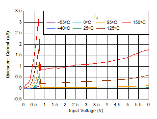
GUID-F5A24EF0-7463-42E9-A275-80B4B7CC02E5-low.gif
VEN = 0.3 V
Figure 6-12 ISHDN vs VIN
GUID-0DC48CB2-764A-49B2-AC6B-DCB3B3B7E541-low.gif
VIN = 2 V
 
Figure 6-14 VEN(HI) and VEN(LOW) Thresholds vs Temperature
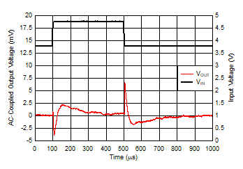
GUID-01964126-9270-4424-B3B0-E4B1E59C7E1C-low.gif
VOUT = 3.3 V, IOUT = 1 mA, slew rate = 1 V/µs
Figure 6-16 Line Transient
GUID-20210317-CA0I-3SMW-VTSB-9C6ZTTDVVNBX-low.gif
VOUT = 3.3 V, IOUT = 1 A, slew rate = 1 V/µs
Figure 6-18 Line Transient vs Temperature
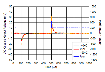
GUID-20210317-CA0I-TF7L-K6D6-FRFRGK62MV7J-low.gif
VOUT = 3.3 V, IOUT = 300 mA to 700 mA, rise time = 1 µs
Figure 6-20 Load Transient vs Temperature
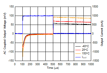
GUID-20210317-CA0I-85P4-GBD9-1GKKFQTWVBCQ-low.gif
VOUT = 3.3 V, IOUT = 0 mA to 1 A, rise time = 1 µs
 
Figure 6-22 Load Transient vs Temperature
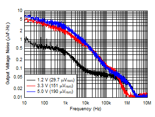
GUID-20210319-CA0I-H72S-6HV8-RVP4DXFK9MFQ-low.gif
IOUT = 1 A
Figure 6-24 Noise vs VOUT
GUID-20210319-CA0I-HBJD-DZMQ-9P6LKXVVCHR6-low.gif
VOUT = 3.3 V, IOUT = 1 A
Figure 6-26 PSRR vs COUT
GUID-EB86EF38-0471-43B8-B414-D5AA56164D2C-low.gif
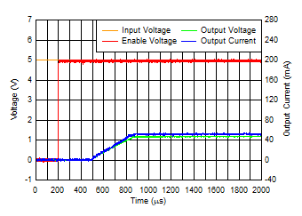
VIN = 5.5 V, CIN = 0 µF, COUT = 1 µF, VOUT = 5.0 V,
IOUT = 0 mA
Figure 6-28 Start-Up Inrush Current With
COUT = 1 µF
GUID-9B0A8F31-09CF-415B-A5FA-171ED54D21BF-low.gif
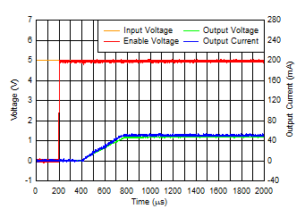
VIN = VEN = 5.5 V, CIN = 0 µF, COUT = 1 µF, VOUT = 1.2 V,
IOUT = 50 mA, TA = 25°C
Figure 6-30 Start Up
GUID-E01271F0-683F-4590-A423-C3221A70C476-low.gif
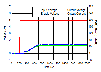
VIN = VEN = 5.5 V, CIN = 0 µF, COUT = 1 µF, VOUT = 5.0 V,
IOUT = 0 mA
Figure 6-32 Start-Up Inrush Current With
COUT = 1 µF
GUID-90D92E3A-2C60-40C5-B92C-79D2C619FDE7-low.gif
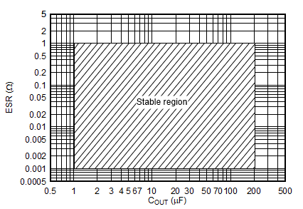
COUT denotes nominal capacitor size
(not effective capacitance)
Figure 6-34 ESR vs COUT