SLVS351Q September   2002  – June 2025 TPS796

PRODUCTION DATA  

  1.   1
  2. Features
  3. Applications
  4. Description
  5. Pin Configuration and Functions
  6. Specifications
    1. 5.1 Absolute Maximum Ratings
    2. 5.2 ESD Ratings
    3. 5.3 Recommended Operating Conditions
    4. 5.4 Thermal Information
    5. 5.5 Electrical Characteristics
    6. 5.6 Typical Characteristics
  7. Detailed Description
    1. 6.1 Overview
    2. 6.2 Functional Block Diagrams
    3. 6.3 Feature Description
      1. 6.3.1 Active Discharge (New Chip)
      2. 6.3.2 Shutdown
      3. 6.3.3 Start-Up
      4. 6.3.4 Undervoltage Lockout (UVLO)
      5. 6.3.5 Regulator Protection
        1. 6.3.5.1 Current Limit
        2. 6.3.5.2 Thermal Shutdown
    4. 6.4 Device Functional Modes
      1. 6.4.1 Normal Operation
      2. 6.4.2 Dropout Operation
      3. 6.4.3 Disabled
  8. Application and Implementation
    1. 7.1 Application Information
      1. 7.1.1 Recommended Capacitor Types
      2. 7.1.2 Input and Output Capacitor Requirements
      3. 7.1.3 Feed-forward Capacitor (CFF)
      4. 7.1.4 Adjustable Configuration
      5. 7.1.5 Load Transient Response
      6. 7.1.6 Dropout Voltage
        1. 7.1.6.1 Exiting Dropout
      7. 7.1.7 Noise Reduction Pin (legacy chip)
      8. 7.1.8 Power Dissipation (PD)
    2. 7.2 Typical Application
      1. 7.2.1 Design Requirements
      2. 7.2.2 Detailed Design Procedure
      3. 7.2.3 Application Curves
      4. 7.2.4 Best Design Practices
    3. 7.3 Power Supply Recommendations
    4. 7.4 Layout
      1. 7.4.1 Layout Guidelines
        1. 7.4.1.1 Board Layout Recommendation to Improve PSRR and Noise Performance
        2. 7.4.1.2 Regulator Mounting
        3. 7.4.1.3 Estimating Junction Temperature
      2. 7.4.2 Layout Examples
  9. Device and Documentation Support
    1. 8.1 Device Support
      1. 8.1.1 Development Support
        1. 8.1.1.1 Evaluation Modules
        2. 8.1.1.2 Spice Models
      2. 8.1.2 Device Nomenclature
    2. 8.2 Documentation Support
      1. 8.2.1 Related Documentation
    3. 8.3 Receiving Notification of Documentation Updates
    4. 8.4 Support Resources
    5. 8.5 Trademarks
    6. 8.6 Electrostatic Discharge Caution
    7. 8.7 Glossary
  10. Revision History
  11. 10Mechanical, Packaging, and Orderable Information

Package Options

Mechanical Data (Package|Pins)
Thermal pad, mechanical data (Package|Pins)
Orderable Information

Load Transient Response

The load-step transient response is the output voltage response by the LDO to a step in load current, whereby output voltage regulation is maintained. There are two key transitions during a load transient response: the transition from a light to a heavy load and the transition from a heavy to a light load. The regions shown in Figure 7-2 are broken down as follows. Regions A, E, and H are where the output voltage is in steady-state.
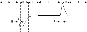
TPS796 Load Transient WaveformFigure 7-2 Load Transient Waveform

During transitions from a light load to a heavy load, the:

  • Initial voltage dip is a result of the depletion of the output capacitor charge and parasitic impedance to the output capacitor (region B)
  • Recovery from the dip results from the LDO increasing the sourcing current, and leads to output voltage regulation (region C)

  • Initial voltage rise results from the LDO sourcing a large current, and leads to the output capacitor charge to increase (region F)
  • Recovery from the rise results from the LDO decreasing the sourcing current in combination with the load discharging the output capacitor (region G)

A larger output capacitance reduces the peaks during a load transient but slows down the response time of the device. A larger DC load also reduces the peaks because the amplitude of the transition is lowered and a higher current discharge path is provided for the output capacitor.