SBVS277C July 2019 – September 2022 TPS7A02
PRODUCTION DATA
- 1 Features
- 2 Applications
- 3 Description
- 4 Revision History
- 5 Pin Configuration and Functions
- 6 Specifications
- 7 Detailed Description
- 8 Application and Implementation
- 9 Device and Documentation Support
- 10Mechanical, Packaging, and Orderable Information
Package Options
Mechanical Data (Package|Pins)
Thermal pad, mechanical data (Package|Pins)
- DQN|4
Orderable Information
3 Description
The TPS7A02 is an ultra-small, ultra-low quiescent current low-dropout linear regulator (LDO) that can source 200 mA with excellent transient performance.
The TPS7A02, with an ultra-low
IQ of 25 nA, is designed specifically for applications
where very-low quiescent current is a critical parameter. This device maintains low
IQ consumption even in dropout mode to further increase battery life.
When in shutdown or disabled mode, the device consumes ultra-low,
3-nA IQ that helps increase the shelf life
of the battery. The TPS7A02 has an output range of 0.8 V to 5.0 V
available in 50-mV steps to support the lower core voltages of modern
microcontrollers (MCUs).
The TPS7A02 features a smart enable circuit with an internally controlled pulldown resistor that keeps the LDO disabled even when the EN pin is left floating and helps minimize the external components used to pulldown the EN pin. This circuit also helps minimize the current drawn through the external pulldown circuit when the device is enabled.
The TPS7A02 is fully specified for TJ = –40°C to +125°C operation.
| PART NUMBER | PACKAGE | BODY SIZE (NOM) |
|---|---|---|
| TPS7A02 | DQN (X2SON, 4) | 1.00 mm × 1.00 mm |
| YCH (DSBGA, 4) | 0.64 mm × 0.64 mm | |
| DBV (SOT-23, 5) | 2.90 mm × 1.60 mm |
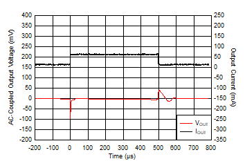
 Load Transient Response
(VIN = VOUT + 1 V, COUT = 1 µF,
IOUT = 1 mA to 50 mA in 1 µs)
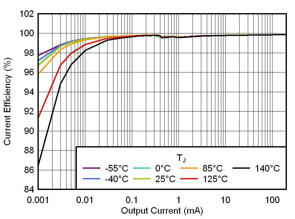
 Ground Current Efficiency vs
Output Current