SBVS375C July   2019  – September 2022 TPS7A03

PRODUCTION DATA  

  1. Features
  2. Applications
  3. Description
  4. Revision History
  5. Pin Configuration and Functions
  6. Specifications
    1. 6.1 Absolute Maximum Ratings
    2. 6.2 ESD Ratings
    3. 6.3 Recommended Operating Conditions
    4. 6.4 Thermal Information
    5. 6.5 Electrical Characteristics
    6. 6.6 Switching Characteristics
    7. 6.7 Typical Characteristics
  7. Detailed Description
    1. 7.1 Overview
    2. 7.2 Functional Block Diagram
    3. 7.3 Feature Description
      1. 7.3.1 Excellent Transient Response
      2. 7.3.2 Active Discharge (P-Version Only)
      3. 7.3.3 Low IQ in Dropout
      4. 7.3.4 Smart Enable
      5. 7.3.5 Dropout Voltage
      6. 7.3.6 Foldback Current Limit
      7. 7.3.7 Undervoltage Lockout (UVLO)
      8. 7.3.8 Thermal Shutdown
    4. 7.4 Device Functional Modes
      1. 7.4.1 Device Functional Mode Comparison
      2. 7.4.2 Normal Operation
      3. 7.4.3 Dropout Operation
      4. 7.4.4 Disabled
  8. Application and Implementation
    1. 8.1 Application Information
      1. 8.1.1 Recommended Capacitor Types
      2. 8.1.2 Input and Output Capacitor Requirements
      3. 8.1.3 Load Transient Response
      4. 8.1.4 Undervoltage Lockout (UVLO) Operation
      5. 8.1.5 Power Dissipation (PD)
        1. 8.1.5.1 Estimating Junction Temperature
        2. 8.1.5.2 Recommended Area for Continuous Operation
    2. 8.2 Typical Application
      1. 8.2.1 Design Requirements
      2. 8.2.2 Detailed Design Procedure
      3. 8.2.3 Application Curve
    3. 8.3 Power Supply Recommendations
    4. 8.4 Layout
      1. 8.4.1 Layout Guidelines
      2. 8.4.2 Layout Examples
  9. Device and Documentation Support
    1. 9.1 Device Support
      1. 9.1.1 Device Nomenclature
    2. 9.2 Receiving Notification of Documentation Updates
    3. 9.3 Support Resources
    4. 9.4 Trademarks
    5. 9.5 Electrostatic Discharge Caution
    6. 9.6 Glossary
  10. 10Mechanical, Packaging, and Orderable Information

Package Options

Mechanical Data (Package|Pins)
Thermal pad, mechanical data (Package|Pins)
Orderable Information

Typical Characteristics

at operating temperature range (TJ = –40°C to +125°C), VIN = VOUT(nom) + 0.5 V or 2.0 V (whichever is greater), IOUT = 1 mA, VEN = VIN, and CIN = COUT = 1 µF (unless otherwise noted)
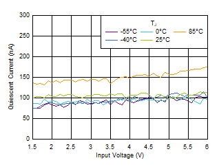
GUID-2FD6590D-CFFE-45D9-920F-B26E26B2BF06-low.gif
VOUT = 1.8 V, VIN = VEN = 2.3 V
Figure 6-1 IQ vs VIN and Temperature
GUID-676894BC-0C78-4534-9A9F-0D4FBA2B4829-low.gif
VOUT = 1.8 V, VIN = VEN = 2.3 V
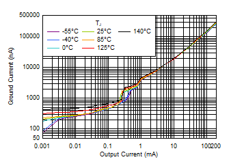
Figure 6-3 IQ vs IOUT and Temperature up to 200 mA
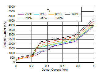
GUID-1DBB1205-88E2-410C-984D-956D33ED536C-low.gif
VOUT = 1.8 V, VIN = VEN = 2.3 V
Figure 6-5 IQ vs IOUT and Temperature Up to 1 mA
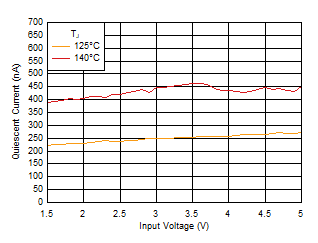
GUID-93D6C6C5-9CC3-4EB4-9D43-F14461743FAF-low.gif
VOUT = 5.0 V, VIN = VEN
Figure 6-7 IQ in Dropout vs VIN and Temperature
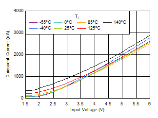
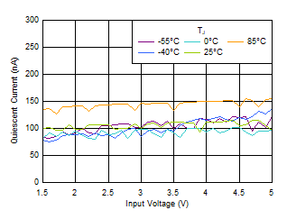
GUID-5E7710B5-FC45-46D8-BC8B-E4C4E0B40B67-low.gif
IOUT = 0 mA, VEN = 1.1 V
Figure 6-9 IQ vs VIN and Temperature
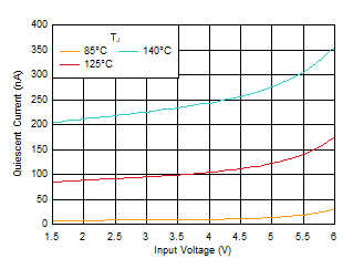
GUID-C3AEBB6A-D09A-41D8-986C-86C3D14F5F04-low.gif
VEN = 0 V
Figure 6-11 ISHDN vs VIN and Temperature
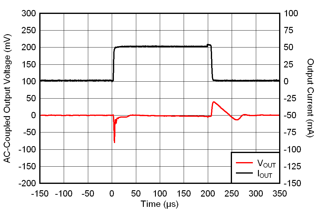
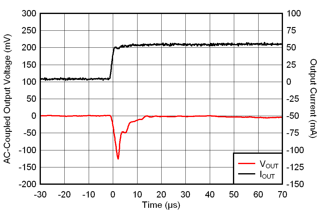
GUID-77A5418F-79BF-471D-A416-256573A449A7-low.gif
VOUT = 1.8 V, VIN = 2.8 V, COUT = 1 µF, tr = tf = 1 µs
Figure 6-13 IOUT Transient From 1 mA to 50 mA
GUID-E20088C3-39DE-4DE4-971F-81F670982D4E-low.gif
VOUT = 1.8 V, VIN = 2.8 V, COUT = 1 µF, tr = tf = 1 µs
Figure 6-15 IOUT Transient From 1 mA to 200 mA
GUID-0128E9D2-2DB1-4AF3-BA50-79A9843F1828-low.gif
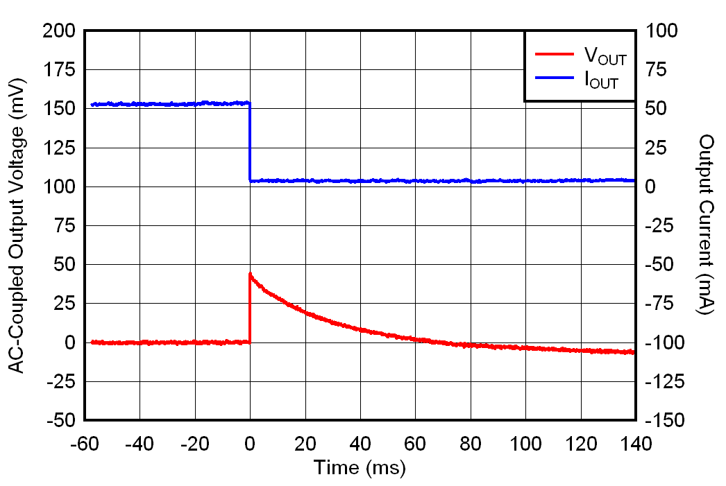
VOUT = 1.8 V, VIN = 2.8 V, COUT = 1 µF, tr = tf = 1 µs
Figure 6-17 IOUT Transient From 50 mA to 0 mA
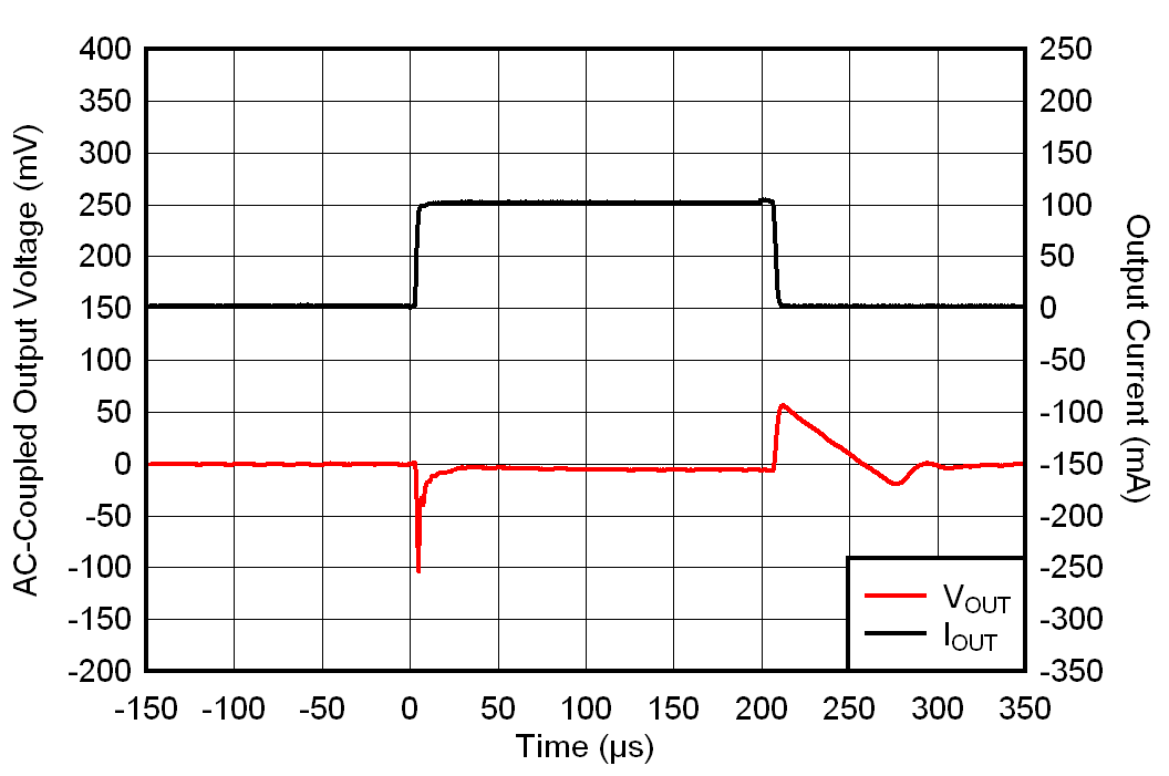
GUID-F66BA38A-8459-4F49-9BCE-C763A3AE449F-low.gif
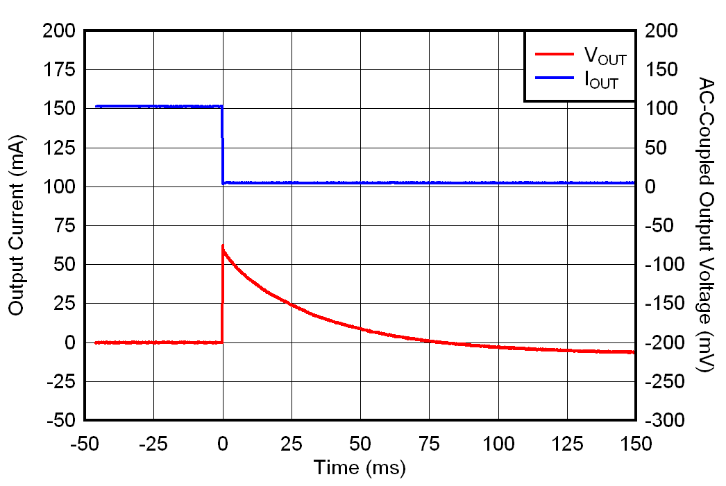
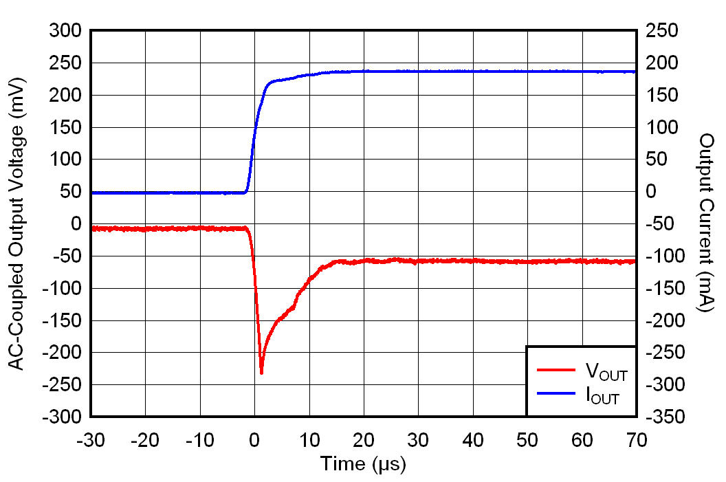
VOUT = 1.8 V, VIN = 2.8 V, COUT = 1 µF, tr = tf = 1 µs
Figure 6-19 IOUT Transient From 100 mA to 0 mA
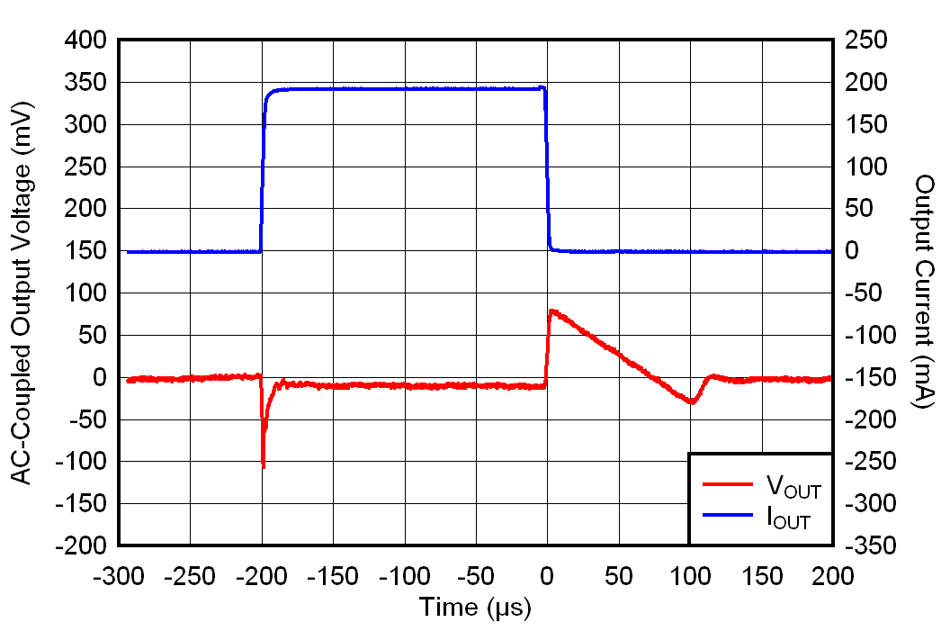
GUID-50082224-2074-4CF6-B6C2-CE4FA88D1069-low.gif
VOUT = 1.8 V, VIN = 2.8 V, COUT = 1 µF, tr = tf = 1 µs
Figure 6-21 IOUT Transient From 200 mA to 0 mA
GUID-D4FF8A2F-A295-45EA-B214-43E4EFBC1112-low.gif
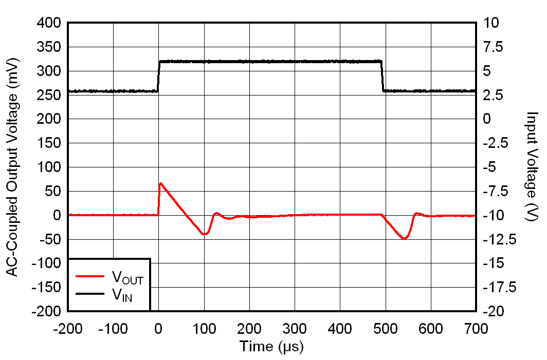
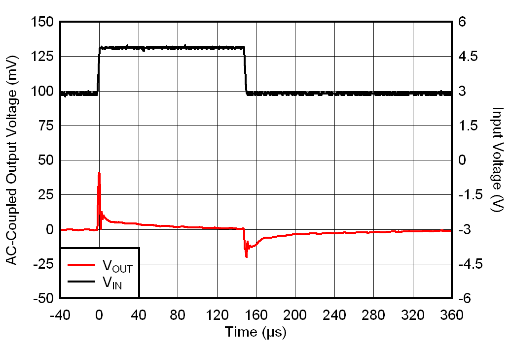
VOUT = 1.8 V, IOUT = 1 mA, COUT = 1 µF, slew rate = 1 V/µs
Figure 6-23 VIN Transient From 2.8 V to 6.0 V
GUID-F30470FC-4F63-4124-9690-55D6425263F7-low.gif
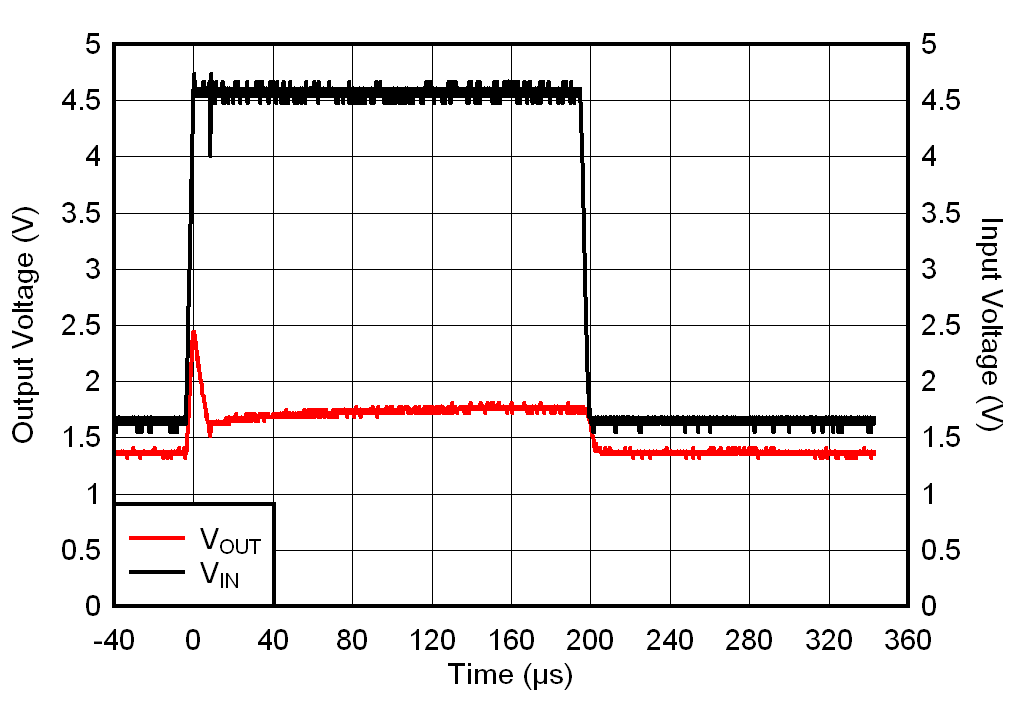
VOUT = 1.8 V, IOUT = 100 mA, COUT = 1 µF, slew rate = 1 V/µs
Figure 6-25 VIN Transient From 1.5 V to 4.5 V
GUID-E703BFB7-4DFD-4A50-BE74-2BDB91984F08-low.gif
VOUT = 1.8 V, IOUT = 1 mA
Figure 6-27 Output Accuracy vs VIN and Temperature
GUID-ADF4B830-B589-49A1-9029-2472B99D827C-low.gif
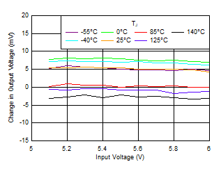
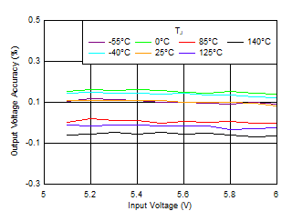
VOUT = 5.0 V, IOUT = 1 mA
Figure 6-29 Line Regulation vs VIN and Temperature
GUID-EF7D3A1E-86DB-4E61-A4AD-83943AB733CA-low.gif
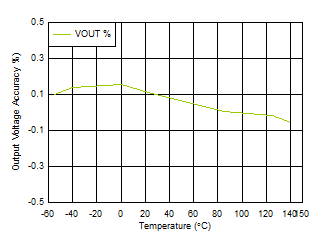
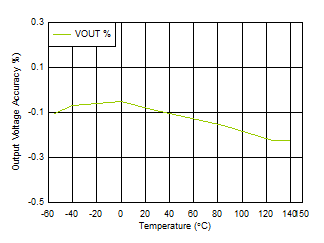
VOUT = 5.0 V, IOUT = 1 mA
Figure 6-31 Output Accuracy vs Temperature
GUID-F8755BAE-285E-4A60-B548-7EA951FEE709-low.gif
VOUT = 1.8 V
Figure 6-33 Dropout vs IOUT and Temperature
GUID-78E78E57-B5DB-45BD-846D-BF7B7D2CAC16-low.gif
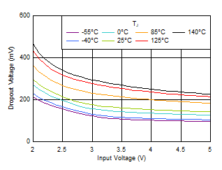
IOUT = 200 mA
Figure 6-35 Dropout vs VIN and Temperature
GUID-336B26E7-815B-48F9-9919-BDC15899F280-low.gif
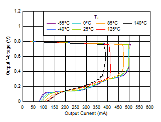
VOUT = 0.8 V
Figure 6-37 Foldback Current Limit vs IOUT and Temperature
GUID-1DE994A1-63F3-42EB-B241-5D4D7F881443-low.gif
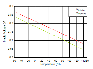
VOUT = 0.8 V
Figure 6-39 EN High and Low Threshold vs Temperature
GUID-22624FCC-E037-44BC-B5DF-FF6C19499E1F-low.gif
VOUT = 5.0 V, IOUT = 1 mA
Figure 6-41 UVLO Rising and Falling Threshold vs Temperature
GUID-285DE85F-42A4-4DCA-8B89-995C3F635F59-low.gif
 
Figure 6-43 Smart Enable Pulldown Resistor vs Temperature and VOUT
GUID-3B7E014F-7800-4305-8DBA-48D4D4F31EDB-low.gif
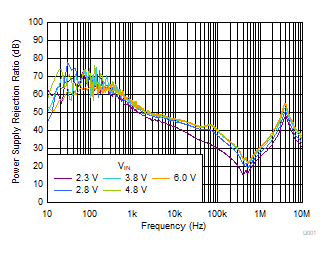
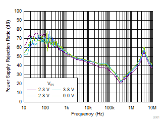
VOUT = 1.8 V, IOUT = 10 mA, COUT = 1 µF
Figure 6-45 PSRR vs Frequency and VIN
GUID-F1F47196-76C8-47BC-83AA-303D48B581B9-low.gif
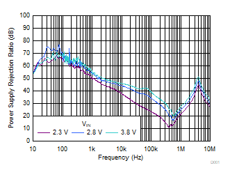
VOUT = 1.8 V, IOUT = 200 mA, COUT = 1 µF
Figure 6-47 PSRR vs Frequency and VIN
GUID-5016FCDD-B7ED-457C-A2D7-A7DFB957B610-low.gif
VOUT = 1.8 V, VIN = 2.8 V, COUT = 1 µF
Figure 6-49 Output Noise vs Frequency and IOUT
GUID-3B462A50-A5CB-431D-974D-0FDB16E00CF0-low.gif
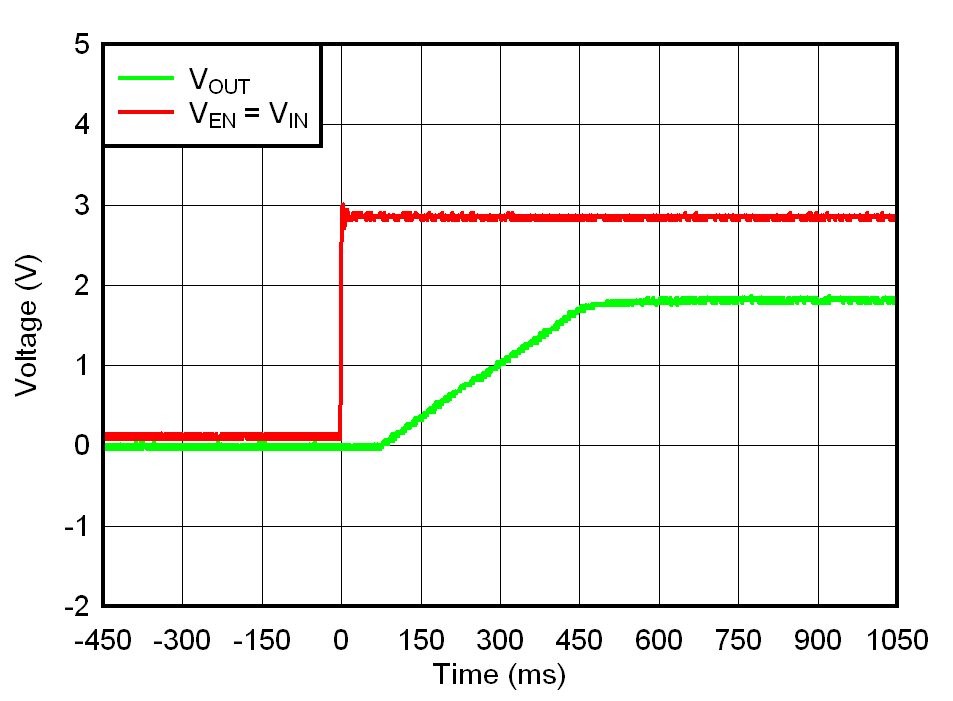
VOUT = 1.8 V, IOUT = 200 mA, COUT = 1 µF
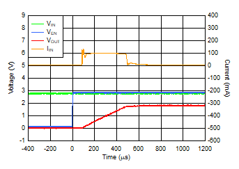
Figure 6-51 Startup With VEN = VIN
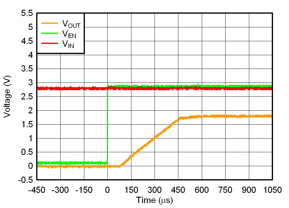
GUID-B566828E-0E98-4D41-ADBA-6E764D19F466-low.gif
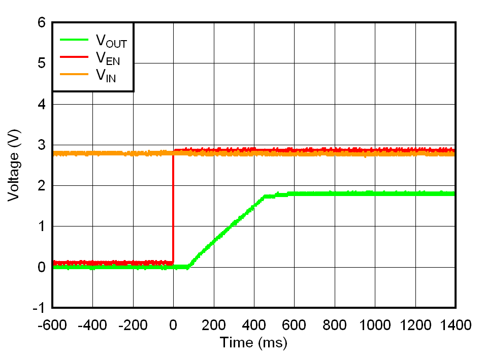
VOUT = 1.8 V, IOUT = 200 mA, COUT = 1 µF
Figure 6-53 Startup With VEN After VIN
GUID-64D6AD45-1326-4ED0-B3F4-19564052121C-low.gif
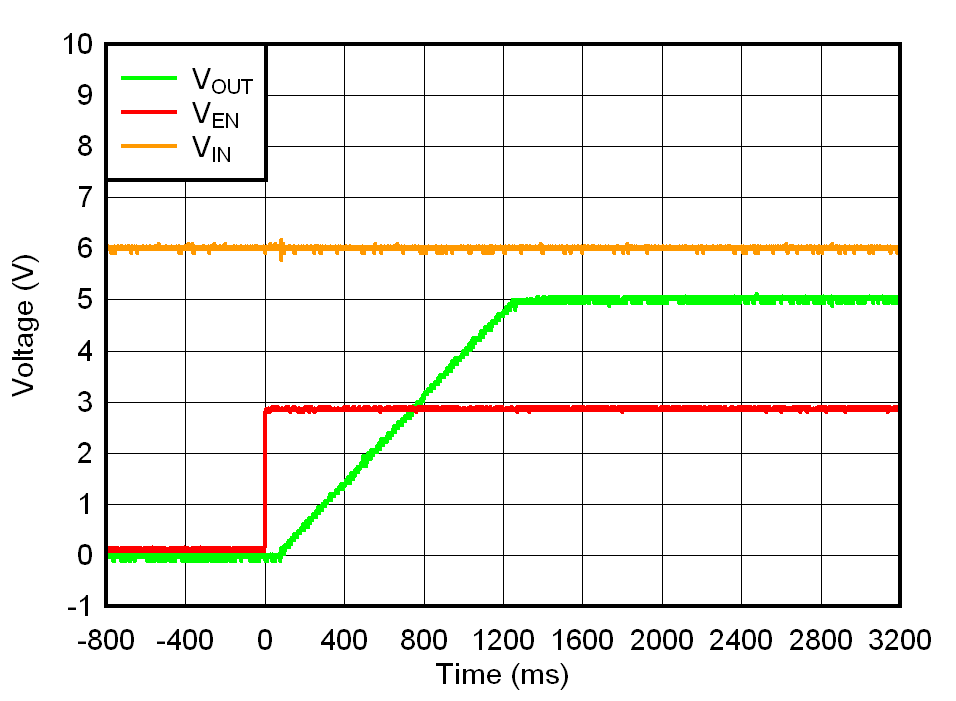
VOUT = 5.0 V, IOUT = 200 mA, COUT = 1 µF
Figure 6-55 Startup With VEN After VIN
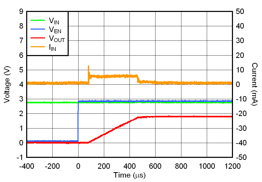
GUID-26AA7D6D-D792-4D76-85B0-DE13466A9B12-low.gif
VOUT = 1.8 V, IOUT = 0 mA
Figure 6-57 Startup Inrush Current With COUT= 22 µF
GUID-5E9318FF-7942-4E3F-BA83-41C3E6396234-low.gif
IOUT = 0 mA, VEN = VIN
Figure 6-2 IQ vs VIN and Temperature
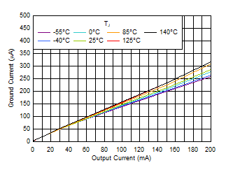
GUID-24BFE2D2-BC07-4AD7-BC61-B80485BF1F5E-low.gif
VOUT = 1.8 V, VIN = VEN = 2.3 V
Figure 6-4 IQ vs IOUT and Temperature Up to 200 mA
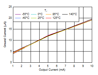
GUID-724A7664-5A0F-49C8-905A-496D122E1165-low.gif
VOUT = 1.8 V, VIN = VEN = 2.3 V
Figure 6-6 IQ vs IOUT and Temperature for 1 mA to 10 mA
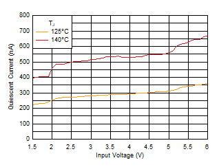
GUID-CEEBDACC-12FE-4BCE-A495-C49317818573-low.gif
VOUT = 5.0 V, VIN = VEN
Figure 6-8 IQ in Dropout vs VIN and Temperature
GUID-A00B2D03-8BA5-4A4C-BC5C-03C16C1BA40A-low.gif
VEN = 0 V
Figure 6-10 ISHDN vs VIN and Temperature
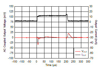
GUID-C8D5B5DA-AEA5-4F6C-A895-F94E579BB6CF-low.gif
VOUT = 1.8 V, VIN = 2.8 V, COUT = 1 µF, tr = tf = 1 µs
Figure 6-12 IOUT Transient From 1 mA to 10 mA
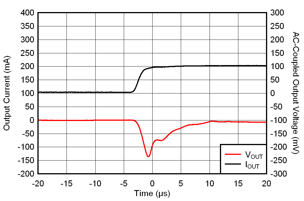
GUID-F1D6524C-36FE-421D-86EE-1A52FBAC16F3-low.gif
VOUT = 1.8 V, VIN = 2.8 V, COUT = 1 µF, tr = tf = 1 µs
Figure 6-14 IOUT Transient From 1 mA to 100 mA
GUID-C56BCE2C-3EC3-428F-8A74-A2B21DFE4411-low.gif
VOUT = 1.8 V, VIN = 2.8 V, COUT = 1 µF, tr = tf = 1 µs
Figure 6-16 IOUT Transient From 0 mA to 50 mA
GUID-AB696D1E-2790-47CF-B7E8-B4D8E7803714-low.gif
VOUT = 1.8 V, VIN = 2.8 V, COUT = 1 µF, tr = tf = 1 µs
Figure 6-18 IOUT Transient From 0 mA to 100 mA
GUID-E30656FA-1014-4987-BA5A-F3F17284A8DE-low.gif
VOUT = 1.8 V, VIN = 2.8 V, COUT = 1 µF, tr = tf = 1 µs
Figure 6-20 IOUT Transient From 0 mA to 200 mA
GUID-B1175727-E1B9-44CE-BF72-77C1CDB96ADF-low.gif
VOUT = 1.8 V, IOUT = 200 mA, COUT = 1 µF, slew rate = 1 V/µs
Figure 6-22 VIN Transient From 2.8 V to 4.8 V
GUID-EA1C1797-BB88-4DCF-9A08-C8DA0220888B-low.gif
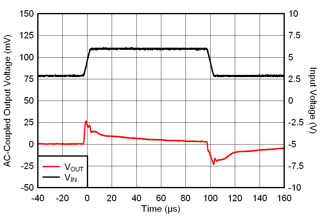
VOUT = 1.8 V, IOUT = 200 mA, COUT = 1 µF, slew rate = 1 V/µs
Figure 6-24 VIN Transient From 2.8 V to 6.0 V
GUID-71AB8D92-85EB-429C-B372-805A11E526AF-low.gif
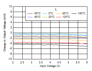
VOUT = 1.8 V, IOUT = 1 mA
Figure 6-26 Line Regulation vs VIN and Temperature
GUID-87487917-CB52-480D-A96E-CEFF81AB5C45-low.gif
VOUT = 1.8 V, IOUT = 1 mA
Figure 6-28 Output Accuracy vs Temperature
GUID-2E492CC3-C250-461A-8DB3-2B550DE6B4FC-low.gif
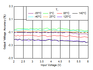
VOUT = 5.0 V, IOUT = 1 mA
Figure 6-30 Output Accuracy vs VIN and Temperature
GUID-B4BEF97A-1E00-4E68-9ADA-DDE47F21CD0F-low.gif
VOUT = 1.8 V
Figure 6-32 Load Regulation vs VIN and Temperature
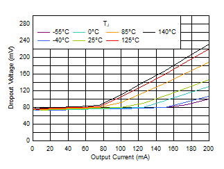
GUID-8646E970-BCF5-4680-A1F8-9EC91C99AB73-low.gif
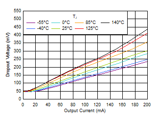
VOUT = 5.0 V
Figure 6-34 Dropout vs IOUT and Temperature
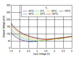
GUID-17DDB131-98A8-4D55-B545-318402D1BAC3-low.gif
IOUT = 50 mA
Figure 6-36 Dropout vs VIN and Temperature
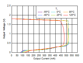
GUID-935C95C0-8A0F-4AE9-8147-269B765D3F80-low.gif
VOUT = 1.8 V
Figure 6-38 Foldback Current Limit vs IOUT and Temperature
GUID-DD45B06D-1CC3-4C55-8322-0152CD9EA5CD-low.gif
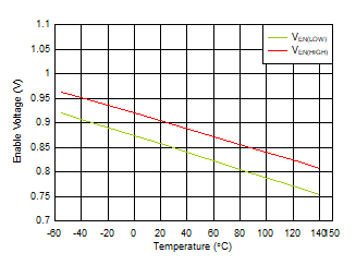
VOUT = 5.0 V
Figure 6-40 EN High and Low Threshold vs Temperature
GUID-07C42C30-B44B-4FEE-94A4-A2D351FC25FC-low.gif
 
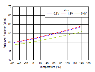
Figure 6-42 Pulldown Resistor vs Temperature and VOUT
GUID-E99C9A1E-D09E-4E7F-8A58-396030AC425C-low.gif
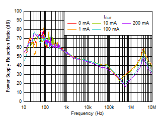
VIN = 2.8 V, VOUT = 1.8 V, COUT = 1 µF
Figure 6-44 PSRR vs Frequency and IOUT
GUID-D0901932-BC1F-4C96-A0C7-553EB1D038C9-low.gif
VOUT = 1.8 V, IOUT = 100 mA, COUT = 1 µF
Figure 6-46 PSRR vs Frequency and VIN
GUID-933AA2E3-E622-4DCC-A01B-49F774C43AD4-low.gif
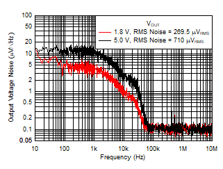
VIN = VOUT+ 1.0 V, IOUT = 1 mA, COUT = 1 µF
Figure 6-48 Output Noise vs Frequency and VOUT
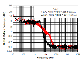
GUID-85CBCCBE-08F5-4D29-A91D-AC7333CF7144-low.gif
VOUT = 1.8 V, VIN = 2.8 V, IOUT = 1 mA
Figure 6-50 Output Noise vs Frequency and COUT
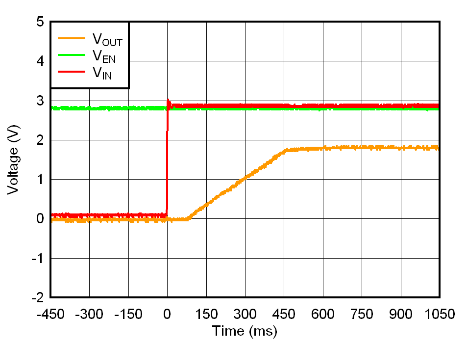
GUID-4C4BE779-6DBF-4D72-B805-C5D5A90FAD11-low.gif
VOUT = 1.8 V, IOUT = 200 mA, COUT = 1 µF
Figure 6-52 Startup With VEN Before VIN
GUID-FDD6574C-5E64-408F-9A18-EC16B567416C-low.gif
VOUT = 1.8 V, IOUT = 0 mA, COUT = 1 µF
Figure 6-54 Startup With VEN After VIN
GUID-A8AF78E8-1056-4695-B88F-A061A78E91E2-low.gif
VOUT = 1.8 V, IOUT = 0 mA
Figure 6-56 Startup Inrush Current With COUT= 1 µF