SBVS399A December   2021  – May 2022 TPS7A13

PRODUCTION DATA  

  1. Features
  2. Applications
  3. Description
  4. Revision History
  5. Pin Configuration and Functions
  6. Specifications
    1. 6.1 Absolute Maximum Ratings
    2. 6.2 ESD Ratings
    3. 6.3 Recommended Operating Conditions
    4. 6.4 Thermal Information
    5. 6.5 Electrical Characteristics
    6. 6.6 Switching Characteristics
    7. 6.7 Typical Characteristics
  7. Detailed Description
    1. 7.1 Overview
    2. 7.2 Functional Block Diagram
    3. 7.3 Feature Description
      1. 7.3.1 Excellent Transient Response
      2. 7.3.2 Global Undervoltage Lockout (UVLO)
      3. 7.3.3 Enable Input
      4. 7.3.4 Internal Foldback Current Limit
      5. 7.3.5 Active Discharge
      6. 7.3.6 Thermal Shutdown
    4. 7.4 Device Functional Modes
      1. 7.4.1 Normal Mode
      2. 7.4.2 Dropout Mode
      3. 7.4.3 Disable Mode
  8. Application and Implementation
    1. 8.1 Application Information
      1. 8.1.1  Recommended Capacitor Types
      2. 8.1.2  Input, Output, and Bias Capacitor Requirements
      3. 8.1.3  Dropout Voltage
      4. 8.1.4  Behavior During Transition From Dropout Into Regulation
      5. 8.1.5  Device Enable Sequencing Requirement
      6. 8.1.6  Load Transient Response
      7. 8.1.7  Undervoltage Lockout Circuit Operation
      8. 8.1.8  Power Dissipation (PD)
      9. 8.1.9  Estimating Junction Temperature
      10. 8.1.10 Recommended Area for Continuous Operation
    2. 8.2 Typical Application
      1. 8.2.1 Design Requirements
      2. 8.2.2 Detailed Design Procedure
      3. 8.2.3 Application Curve
  9. Power Supply Recommendations
  10. 10Layout
    1. 10.1 Layout Guidelines
    2. 10.2 Layout Example
  11. 11Device and Documentation Support
    1. 11.1 Device Support
      1. 11.1.1 Development Support
        1. 11.1.1.1 Evaluation Module
      2. 11.1.2 Device Nomenclature
    2. 11.2 Documentation Support
      1. 11.2.1 Related Documentation
    3. 11.3 Receiving Notification of Documentation Updates
    4. 11.4 Support Resources
    5. 11.5 Trademarks
    6. 11.6 Electrostatic Discharge Caution
    7. 11.7 Glossary
  12. 12Mechanical, Packaging, and Orderable Information
    1. 12.1 Mechanical Data

Package Options

Refer to the PDF data sheet for device specific package drawings

Mechanical Data (Package|Pins)
  • YCK|6
Thermal pad, mechanical data (Package|Pins)
Orderable Information

Typical Characteristics

at operating temperature TJ = 25°C, VOUT(NOM) = 0.9 V, VIN = VOUT(NOM) + 0.1 V, VBIAS = VOUT(NOM) + 1.4 V, IOUT = 1 mA, VEN = VIN, CIN = 1 µF, COUT = 1 µF, and CBIAS = 0.1 µF (unless otherwise noted)

GUID-20211210-SS0I-HLJ9-PXR3-SM7GGPG8KHLJ-low.jpg
 
Figure 6-1 Output Voltage Accuracy vs VIN
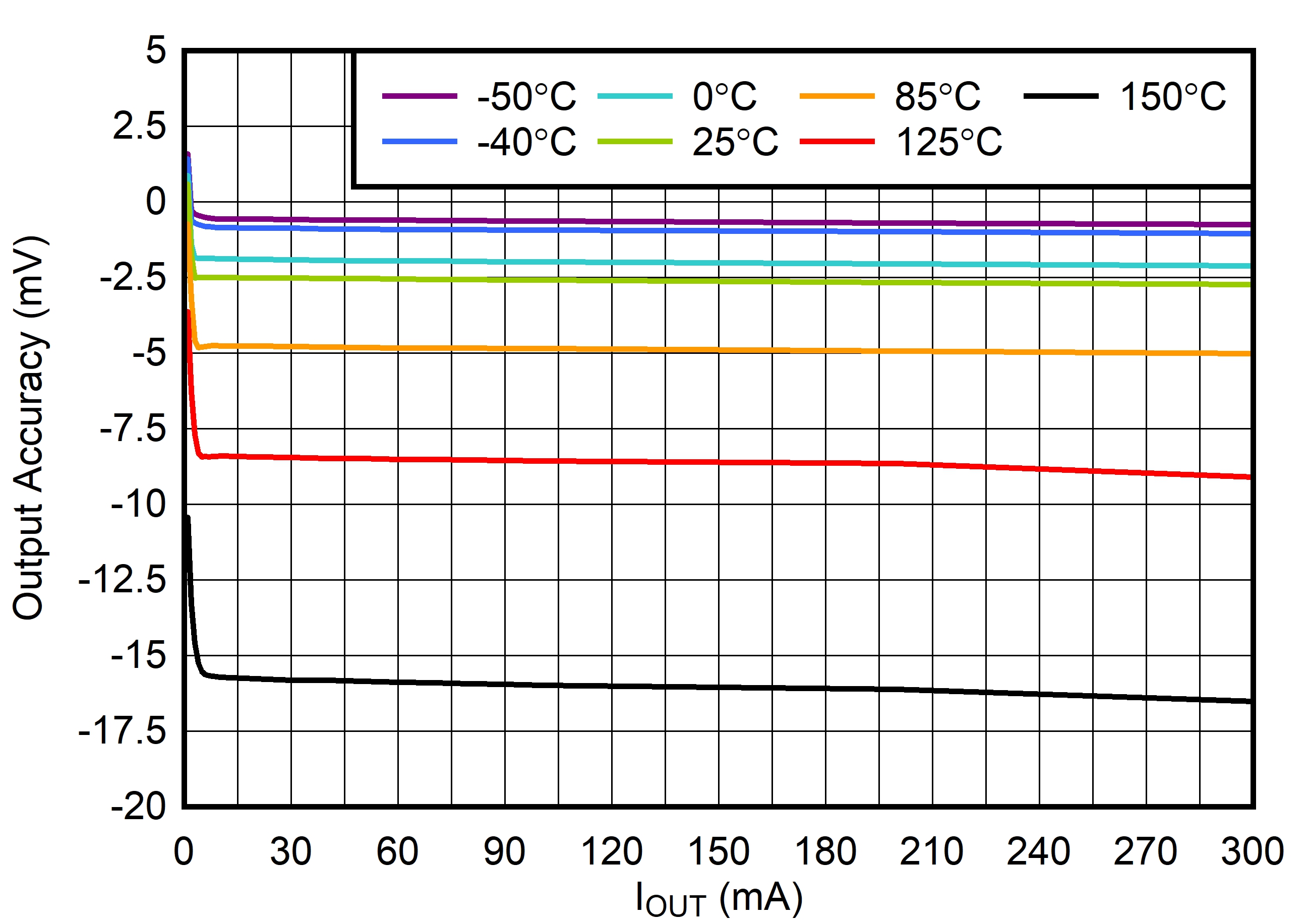
GUID-20211210-SS0I-F36W-D1CD-H9SJ3LQ08BP8-low.jpg
 
Figure 6-3 Output Voltage Accuracy vs IOUT
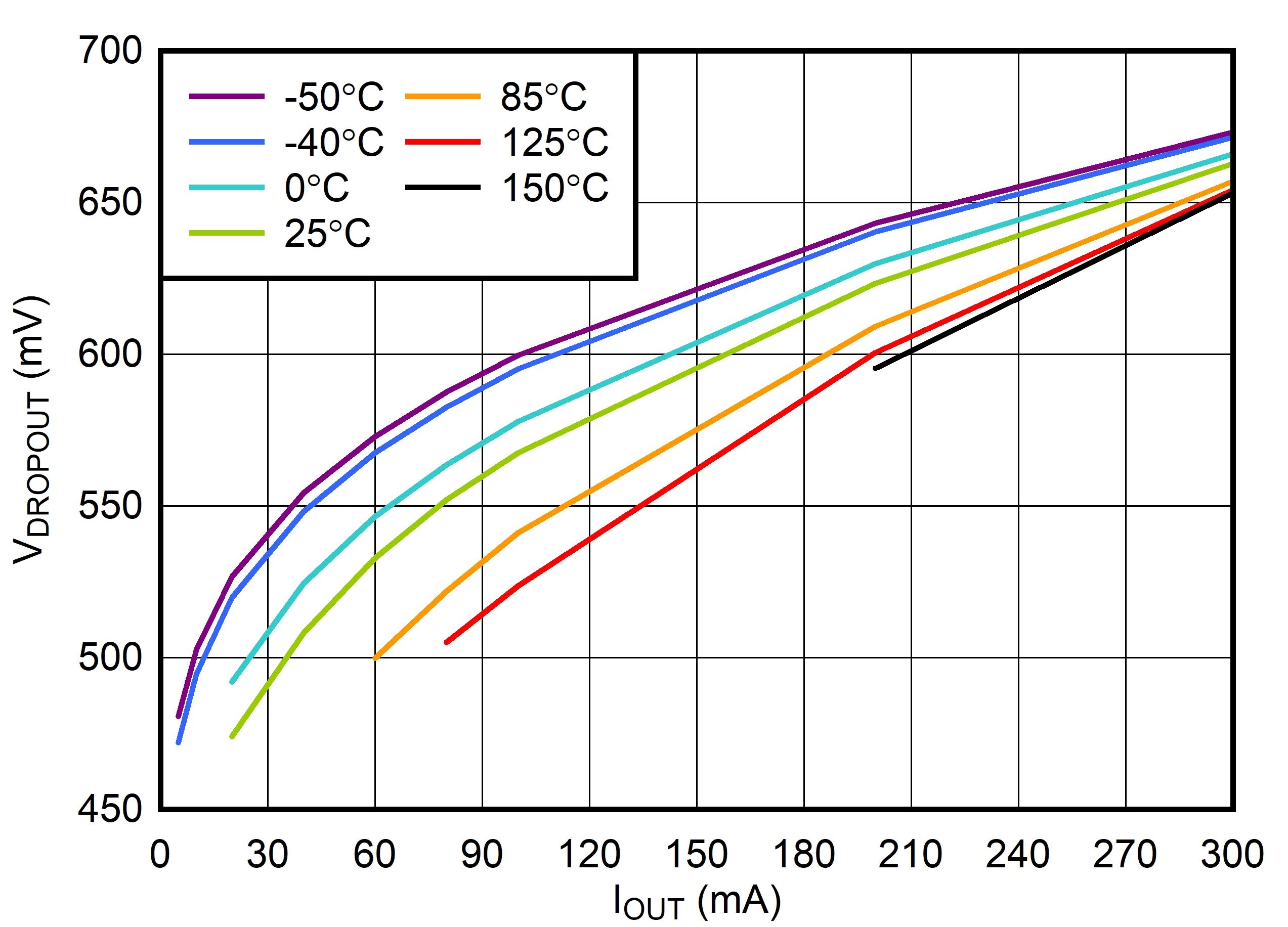
GUID-20211210-SS0I-DBDF-XNRF-KLN3GFDB0LTS-low.jpg
 
Figure 6-5 VBIAS Dropout Voltage vs IOUT
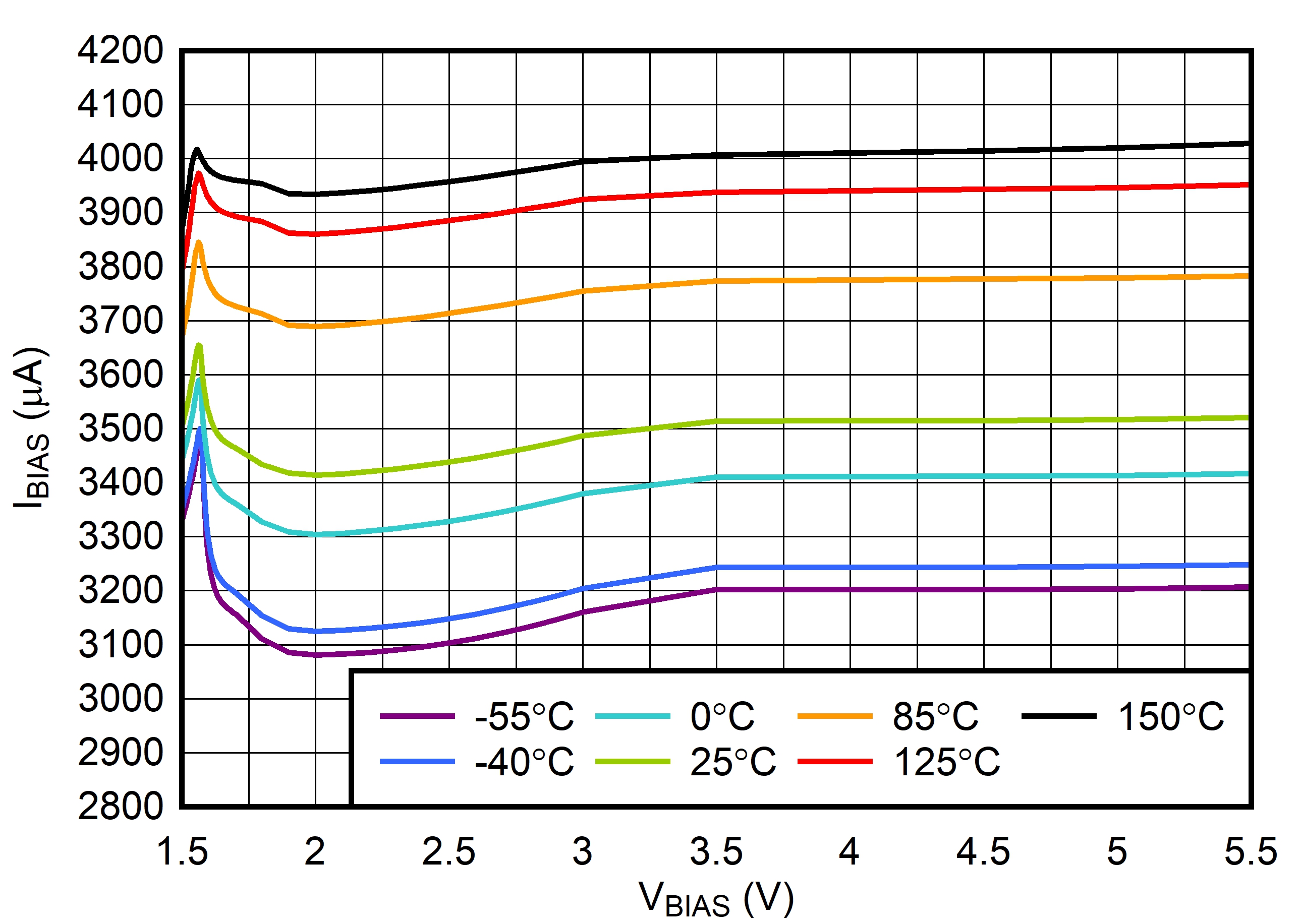
GUID-20211210-SS0I-56J3-CBJN-DWPQNJC81LVC-low.jpg
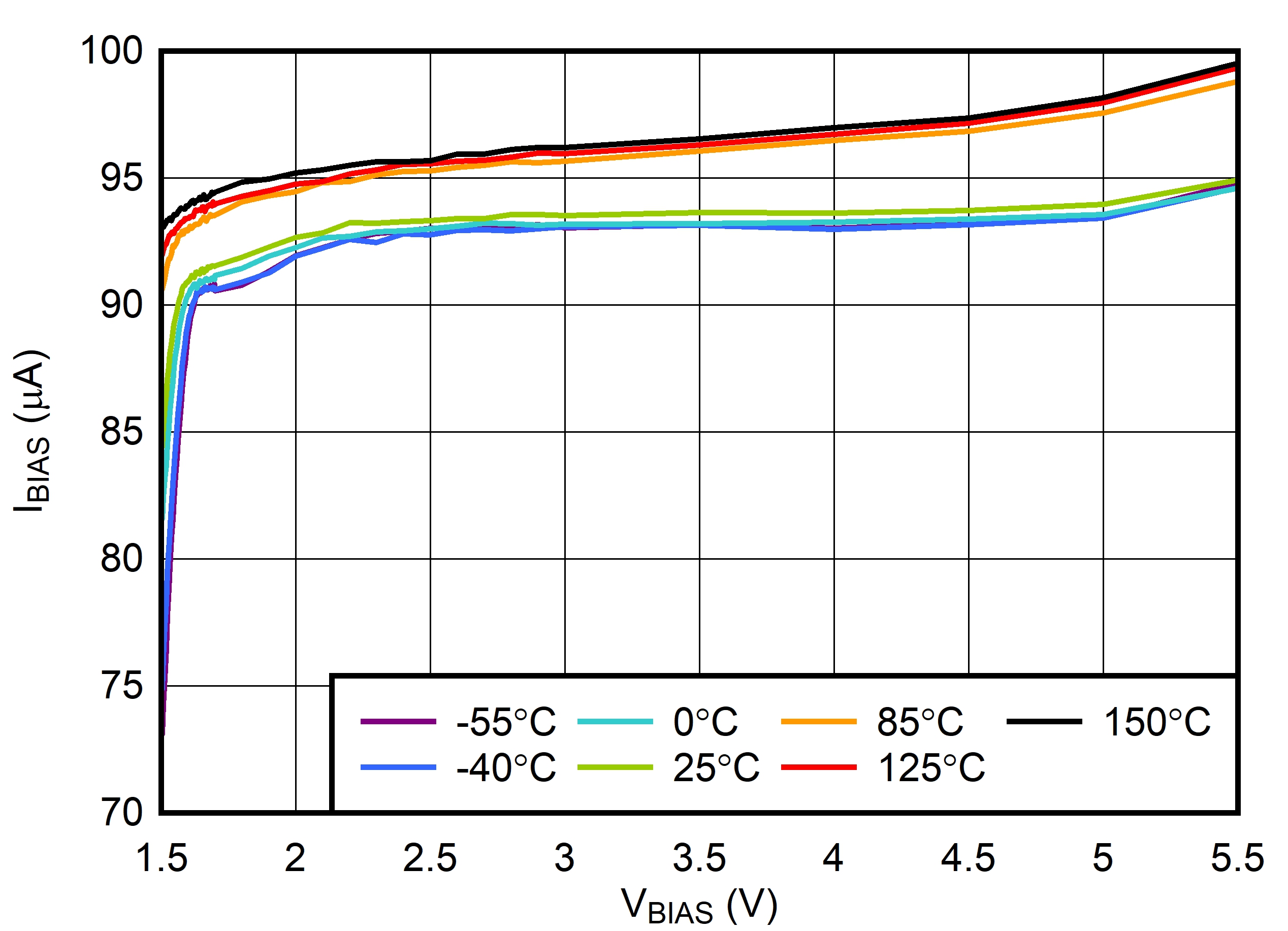
IOUT = 300 mA
Figure 6-7 VBIAS Input Current vs VBIAS
GUID-20211210-SS0I-7N2T-7PSR-LRK6QGQXZMBS-low.jpg
IOUT = 0 mA
Figure 6-9 VBIAS Shutdown IQ vs VBIAS
GUID-20211210-SS0I-L39J-RBPC-SVJHRFKZQ4FL-low.jpg
 
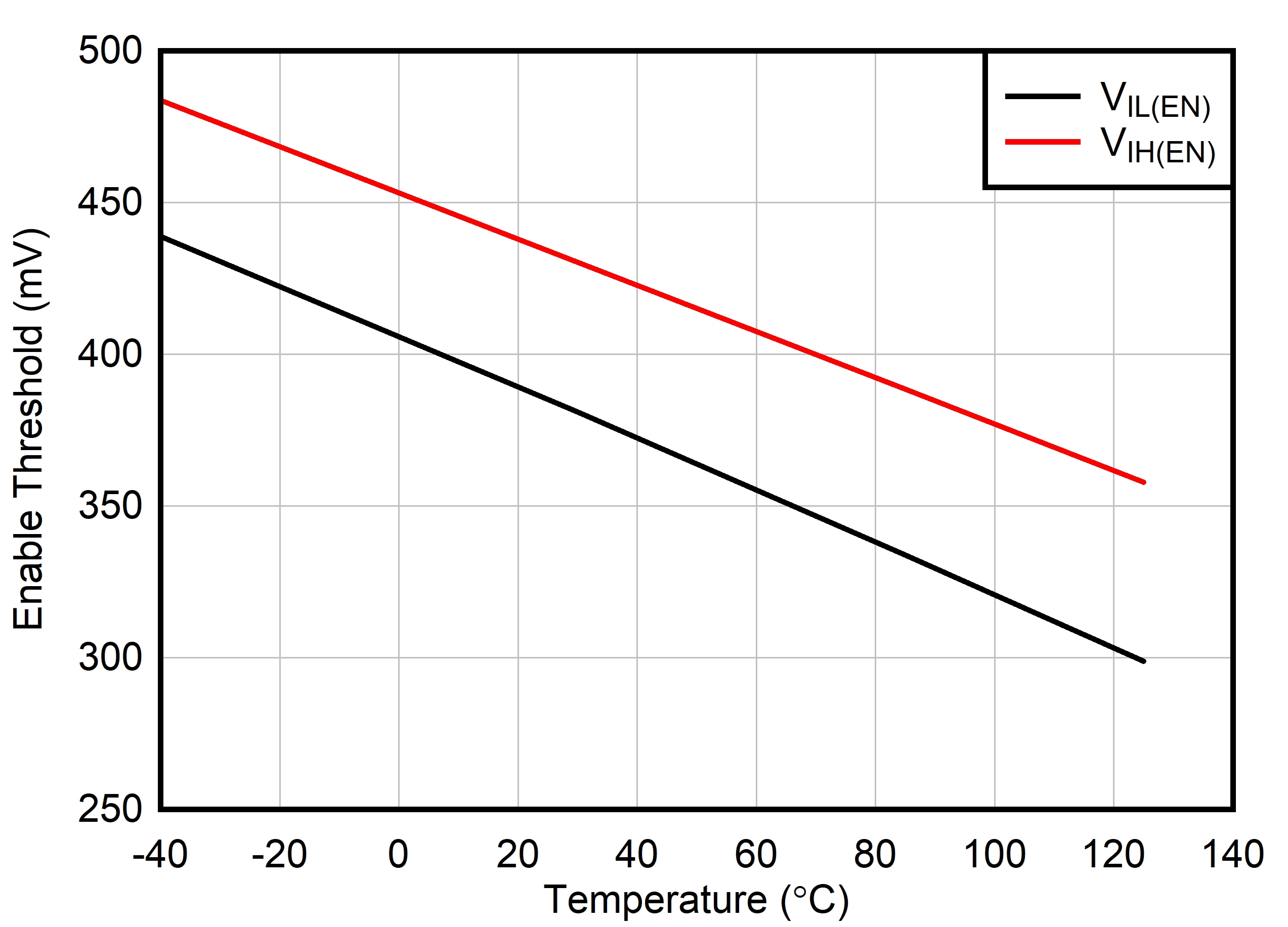
Figure 6-11 Enable Threshold vs Temperature
GUID-20211210-SS0I-ZRTX-RLX4-LJ2DRHLRQVN0-low.jpg
 
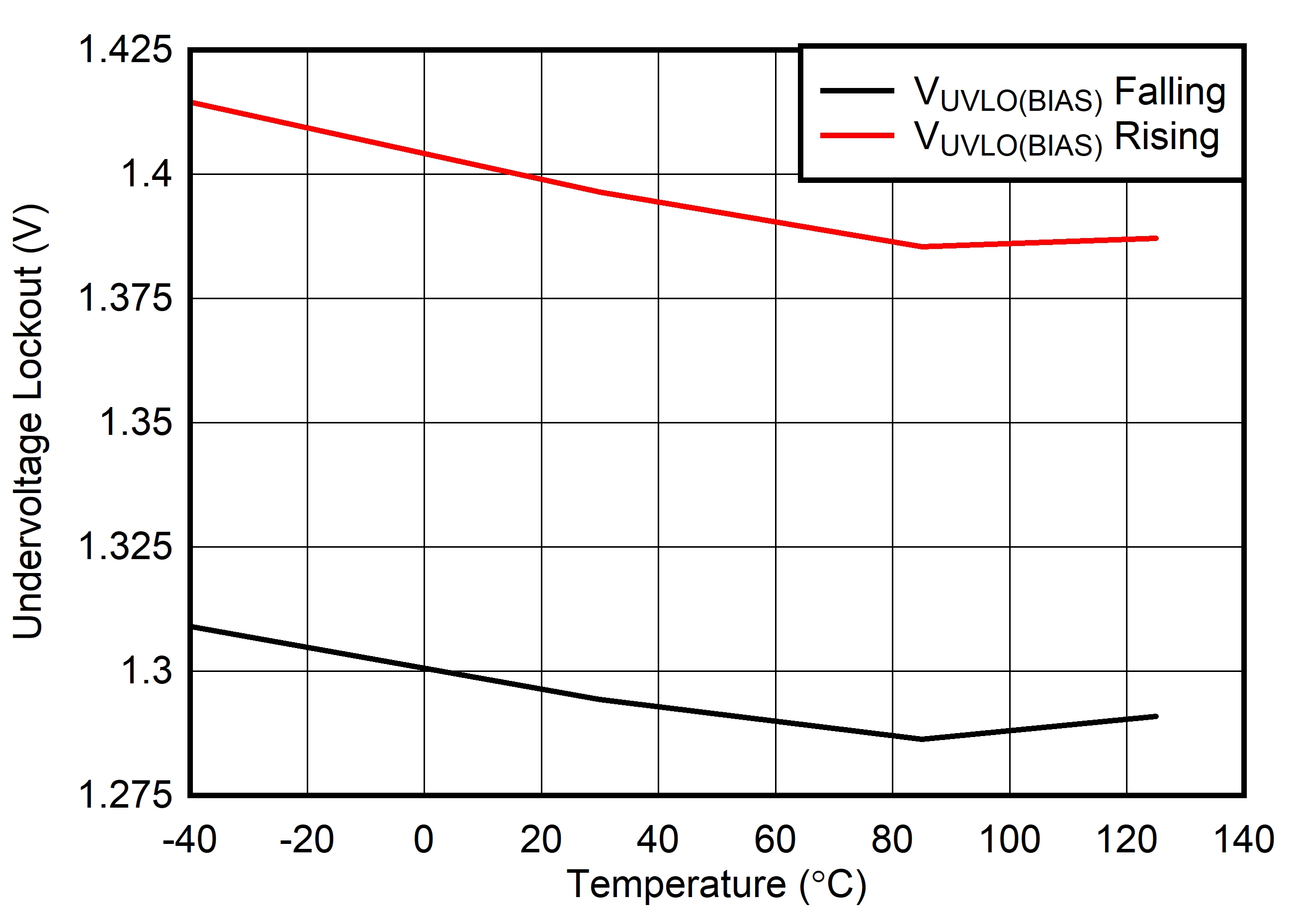
Figure 6-13 VBIAS UVLO vs Temperature
GUID-20211210-SS0I-VP8Q-NVWV-2WNQFLTVC1J3-low.jpg
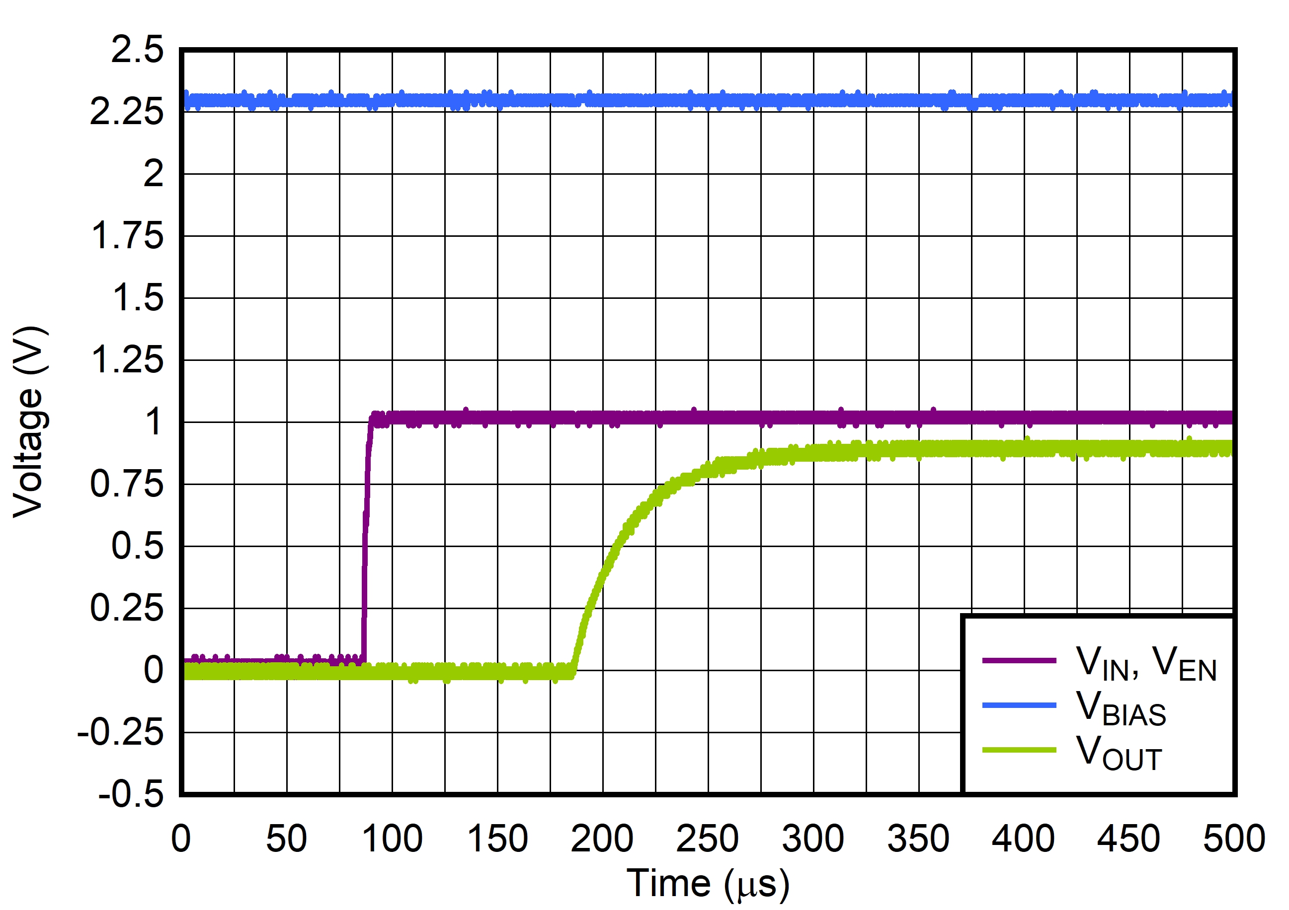
tr = 1 μs
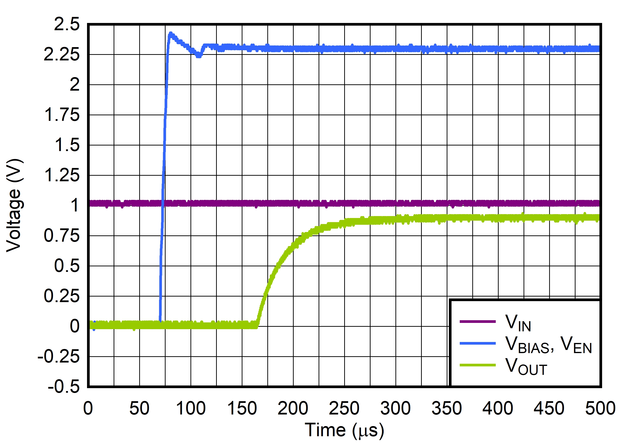
Figure 6-15 Start-Up With VIN Before VBIAS and VEN
GUID-20211210-SS0I-GTHL-6T0L-ZZ8D9CG6XZDC-low.jpg
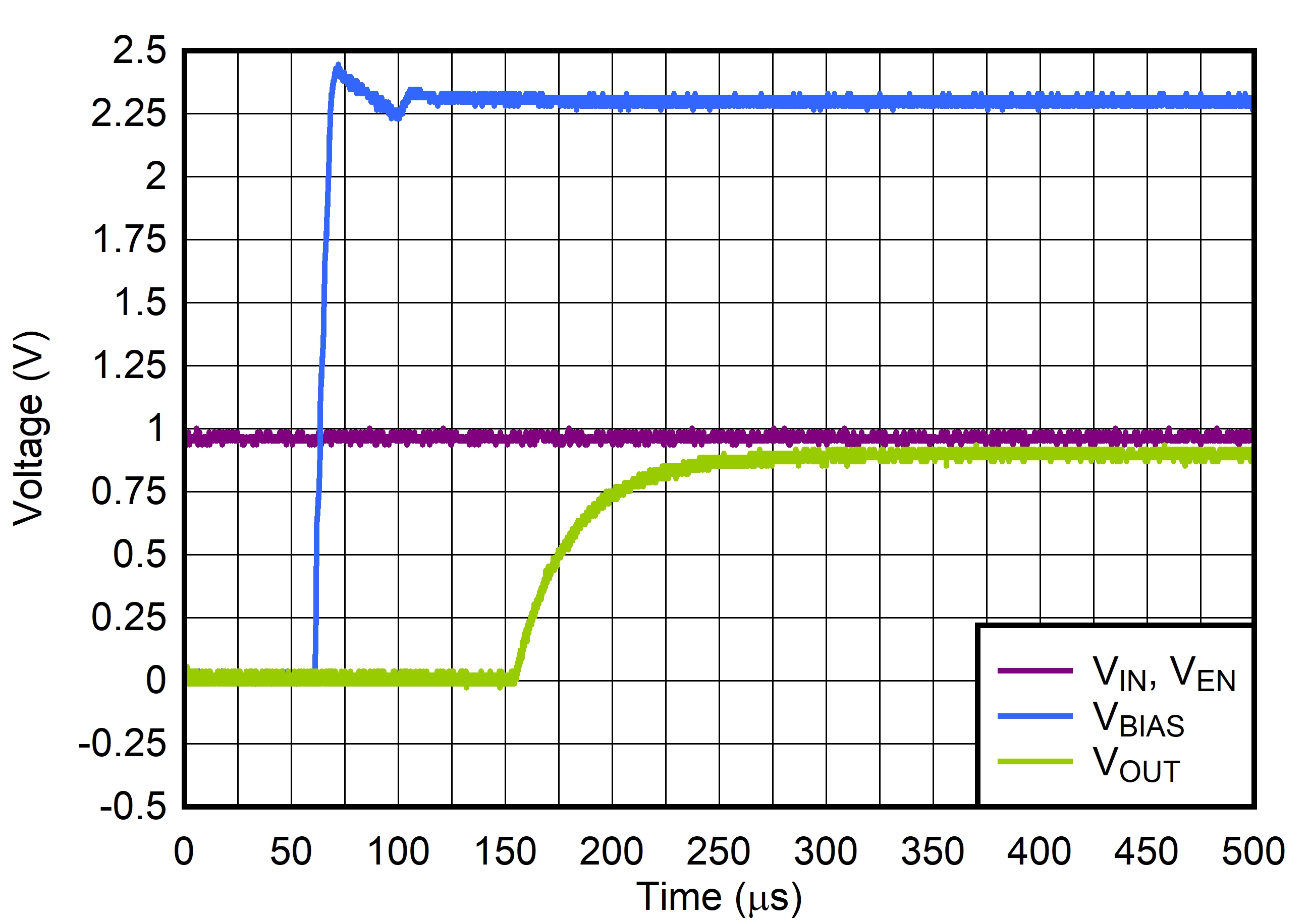
tr = 1 μs
Figure 6-17 Start-Up With VIN and VEN Before VBIAS
GUID-20211210-SS0I-PPDJ-LRH3-KSHXDMWCCSMD-low.jpg
tr = tf = 1 μs, IOUT = 300 mA
Figure 6-19 Line Transient From 1 V to 2.2 V
GUID-20211210-SS0I-GXRX-V7RQ-LJF3HSMBWSLN-low.jpg
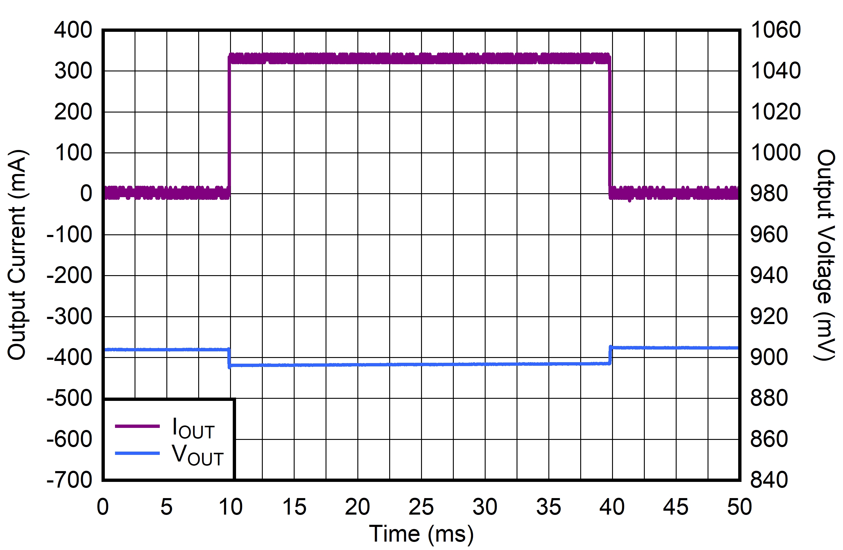
tr = tf = 20 μs
 
Figure 6-21 Load Transient From 100 μA to 320 mA
GUID-20211210-SS0I-1WZD-LT4N-FW0MGWF95VQL-low.jpg
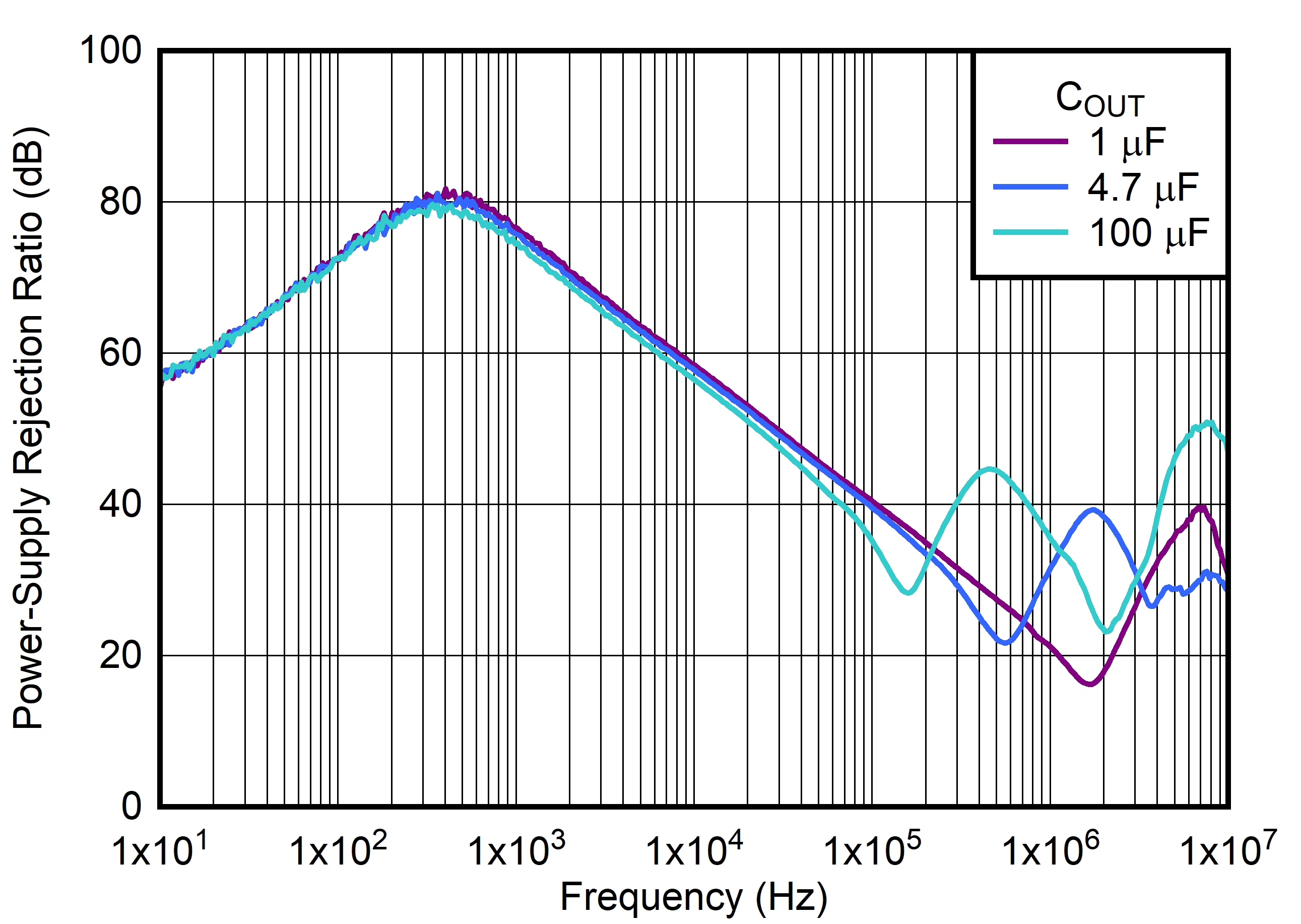
CBIAS = 0 μF, IOUT = 300 mA
Figure 6-23 VIN PSRR vs Frequency and COUT
GUID-20211210-SS0I-WKSC-KKCW-RXVRFFJVVTV4-low.jpg
CBIAS = 0 μF
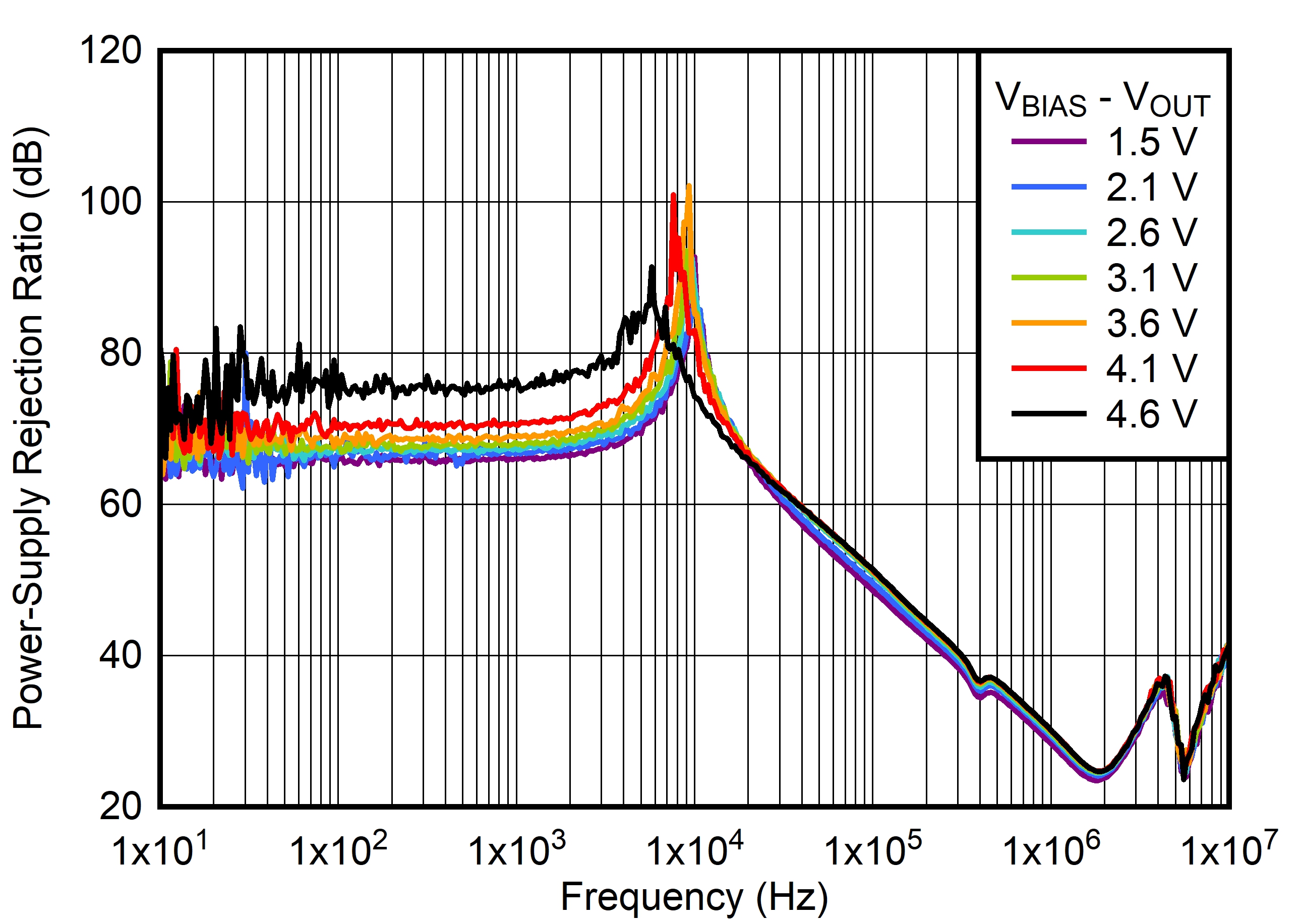
Figure 6-25 VBIAS PSRR vs Frequency and VBIAS – VOUT
GUID-20211210-SS0I-HCM9-VCZ7-7CW3B7BSCDSC-low.jpg
 
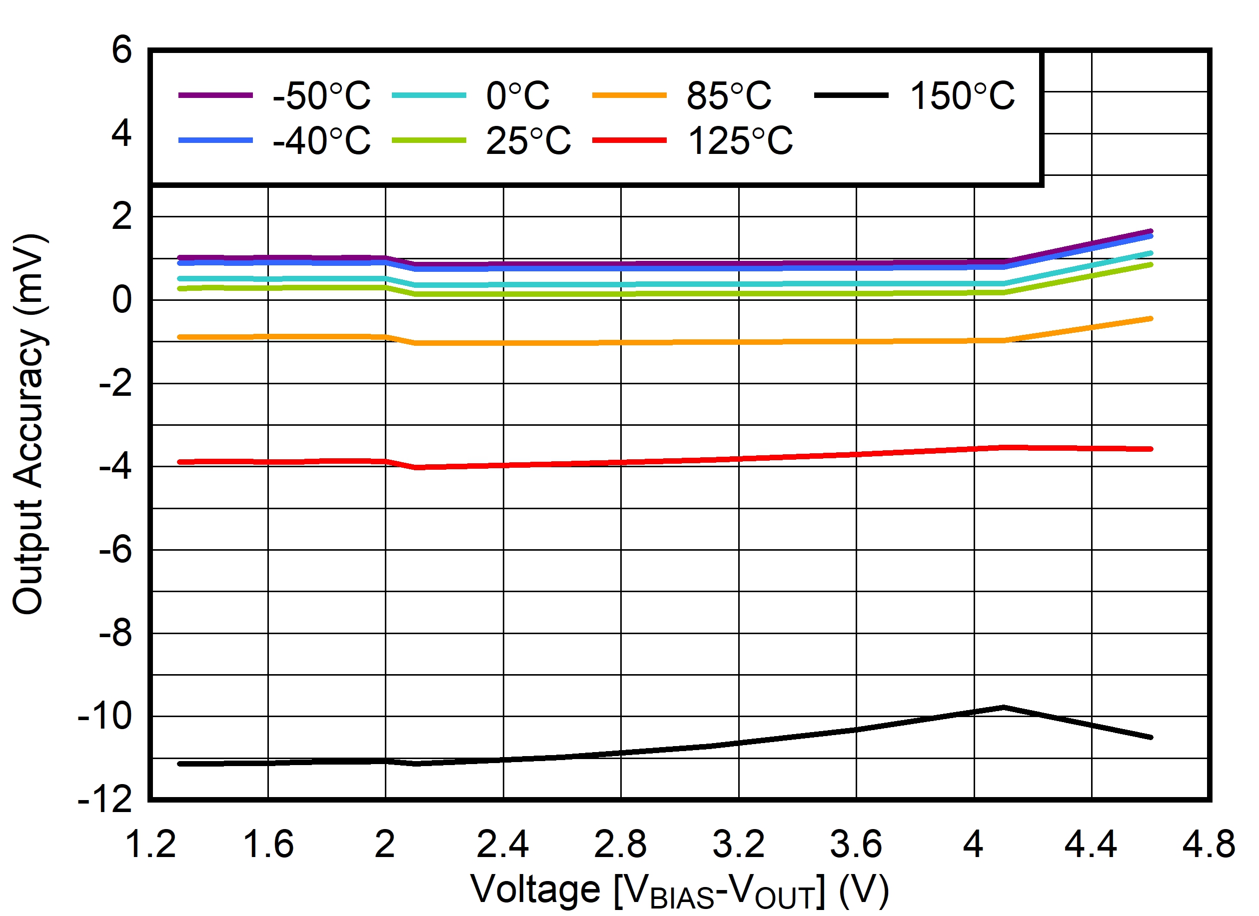
Figure 6-2 Output Voltage Accuracy vs VBIAS
GUID-20211210-SS0I-KDKV-LC44-XKSGB7MJPRJC-low.jpg
 
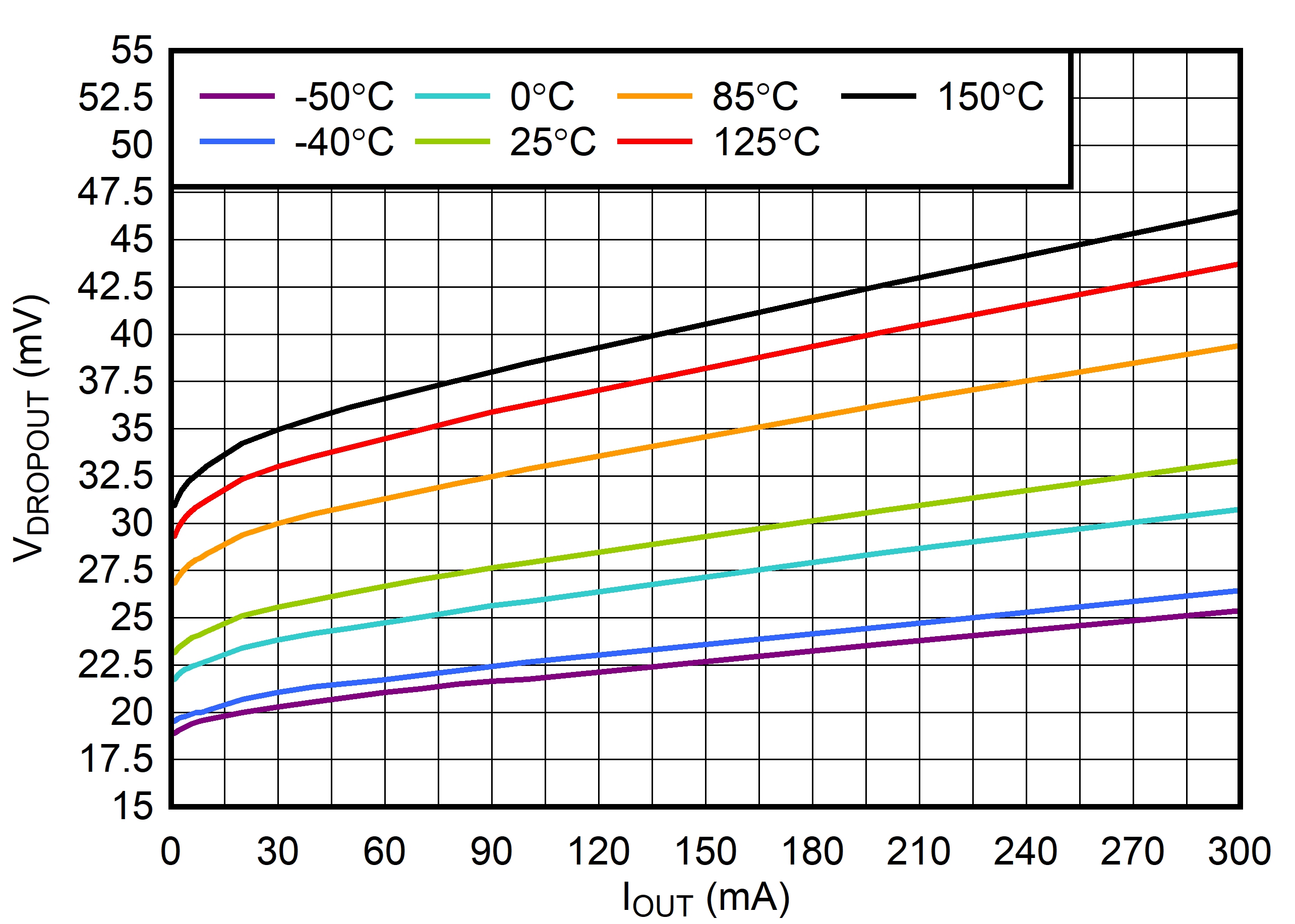
Figure 6-4 VIN Dropout Voltage vs IOUT
GUID-20211210-SS0I-0CJN-J8TM-5MXMGGHH07XL-low.jpg
 
Figure 6-6 VBIAS Input Current vs VBIAS
GUID-20211210-SS0I-0KCZ-DD6S-WJP5LRWK634N-low.jpg
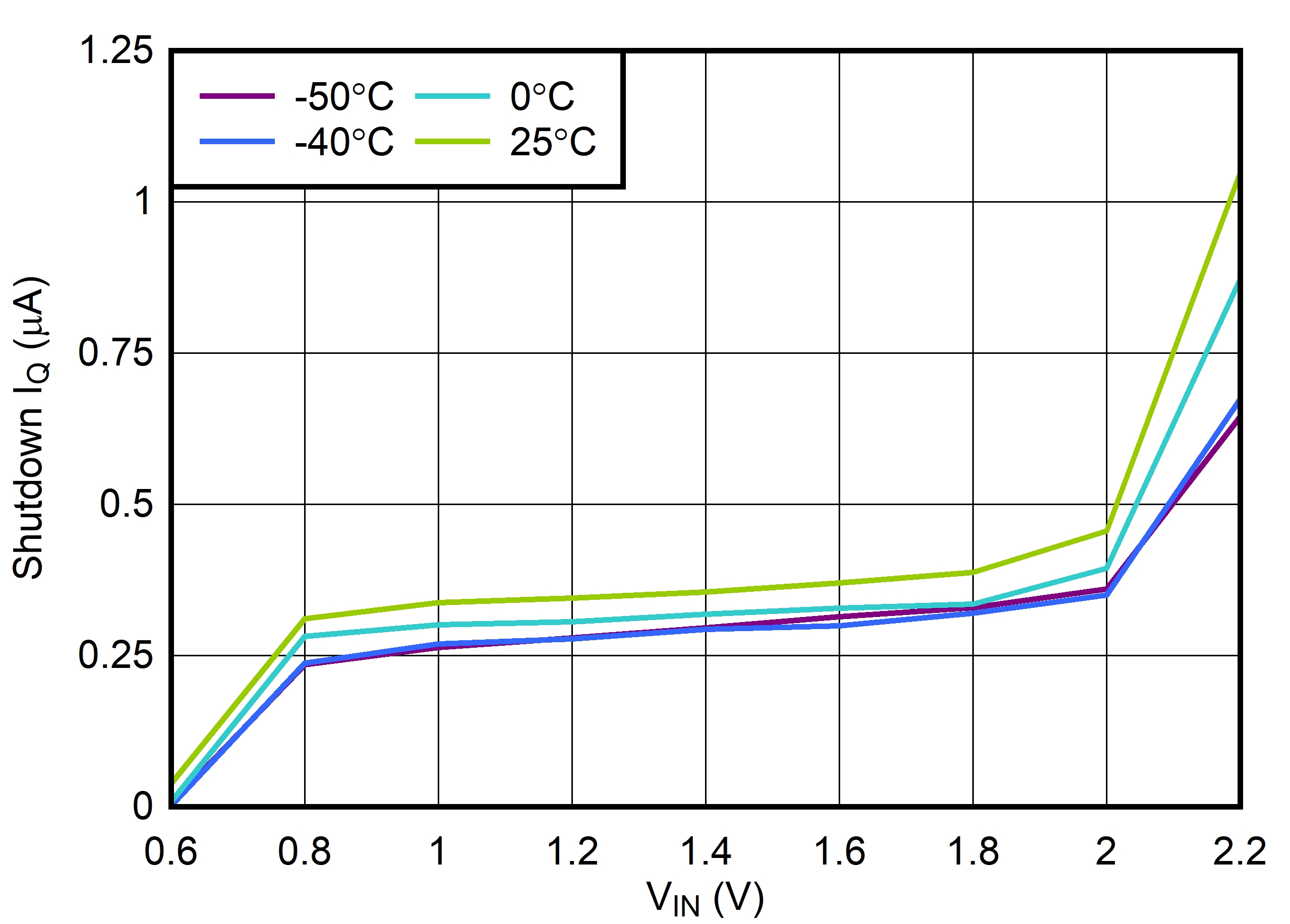
IOUT = 0 mA
Figure 6-8 VIN Shutdown IQ vs VIN
GUID-20211210-SS0I-HQ79-GPW6-1SCZS0XKMZRG-low.jpg
 
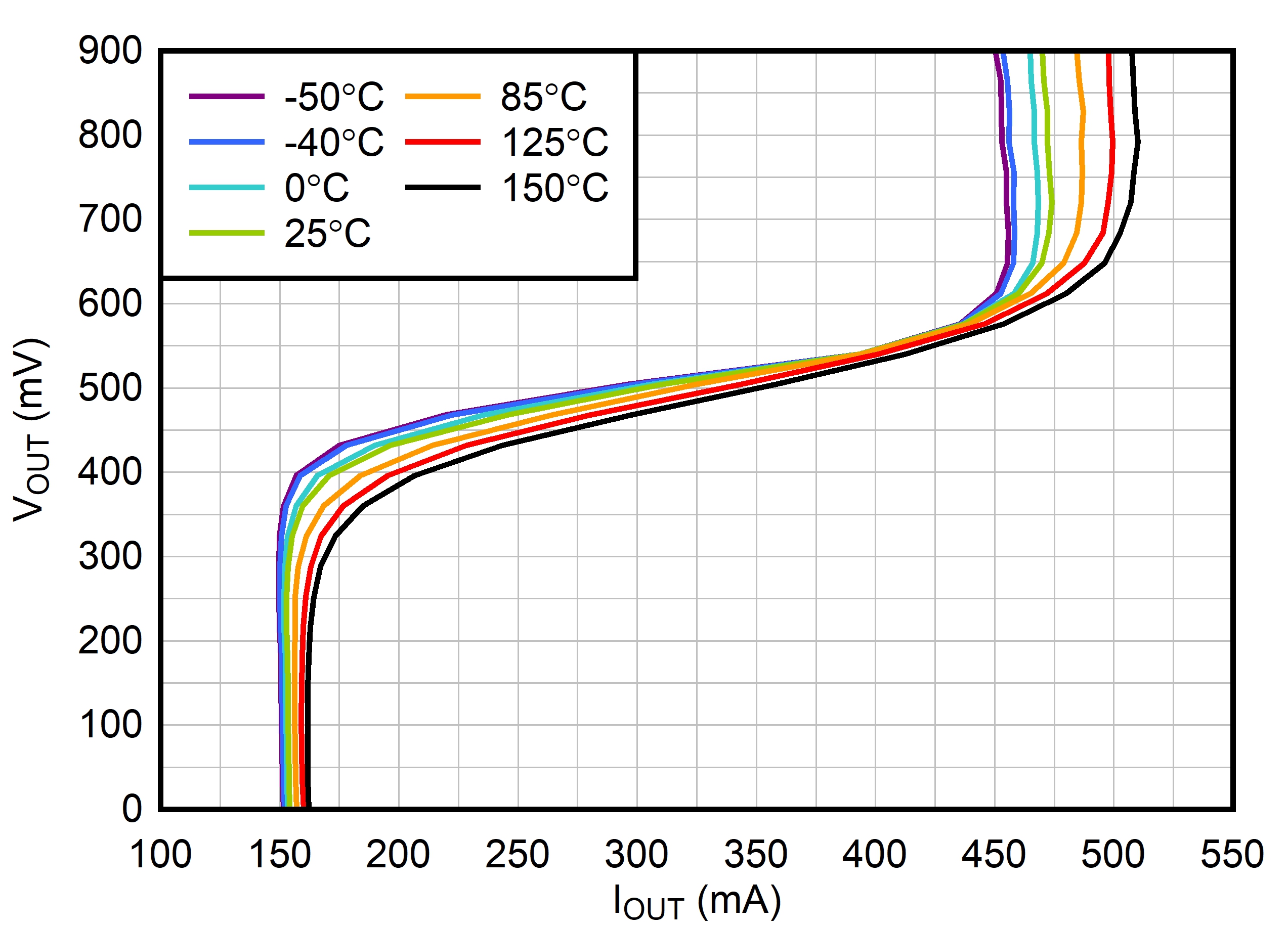
Figure 6-10 Foldback Current Limit vs IOUT
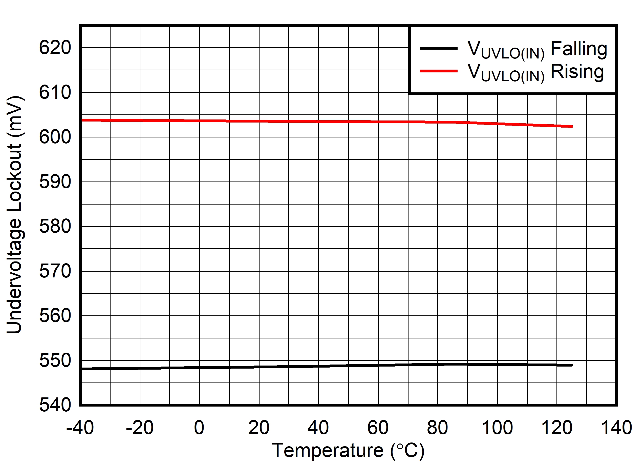
GUID-20211210-SS0I-BS5X-P4SC-MLRK5Z96TR6K-low.jpg
 
Figure 6-12 VIN UVLO vs Temperature
GUID-20211210-SS0I-KJBN-BLZM-ZNGBCPZ9JKV1-low.jpg
tr = 1 μs
Figure 6-14 Start-Up With VBIAS Before VIN
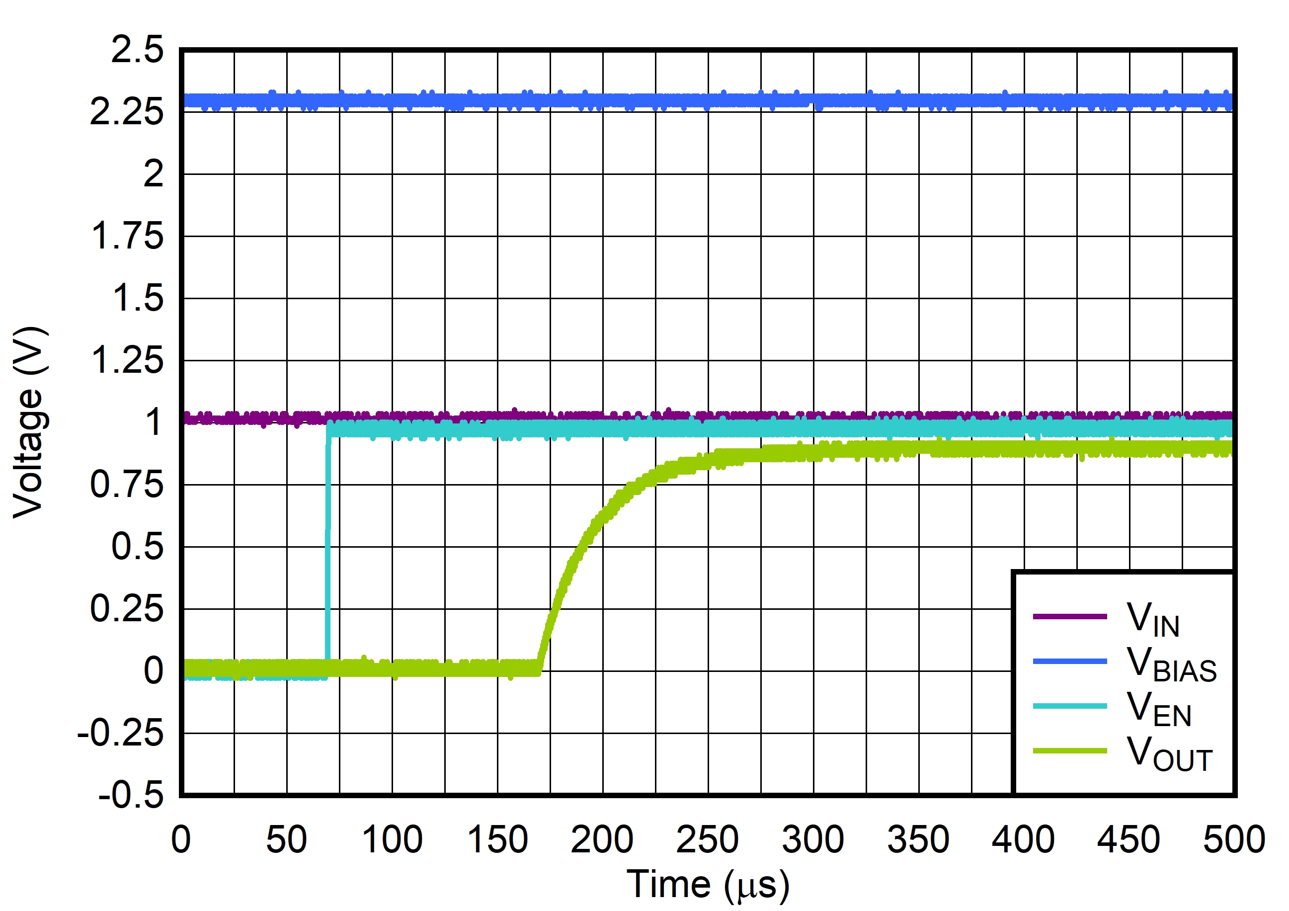
GUID-20211210-SS0I-PWNH-P0LQ-T50VX5NHLVXL-low.jpg
tr = 1 μs
Figure 6-16 Start-Up With VIN and VBIAS Before VEN
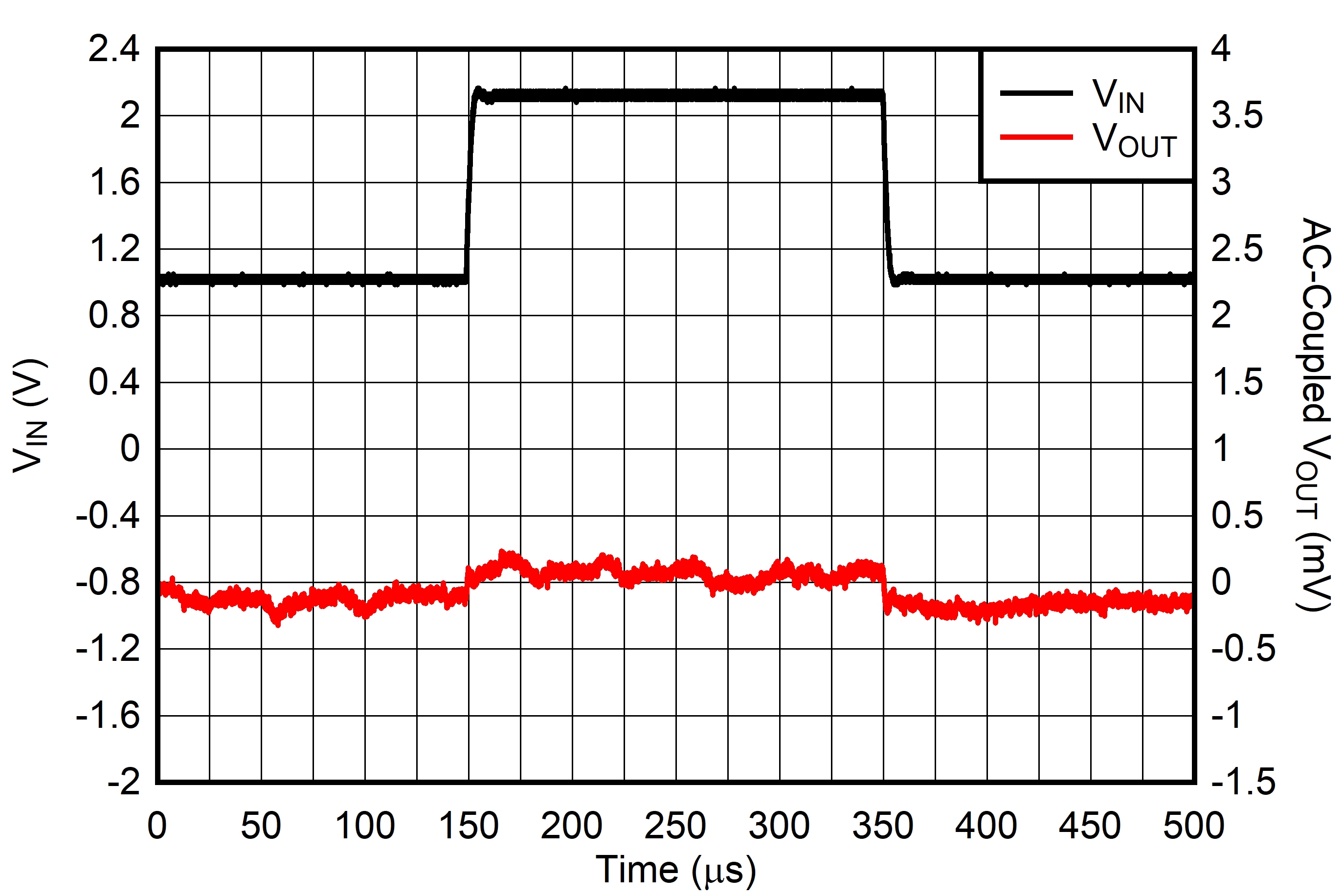
GUID-20211210-SS0I-MPTT-56GW-QHRPD73WCP1C-low.jpg
tr = tf = 1 μs
Figure 6-18 Line Transient From 1 V to 2.2 V
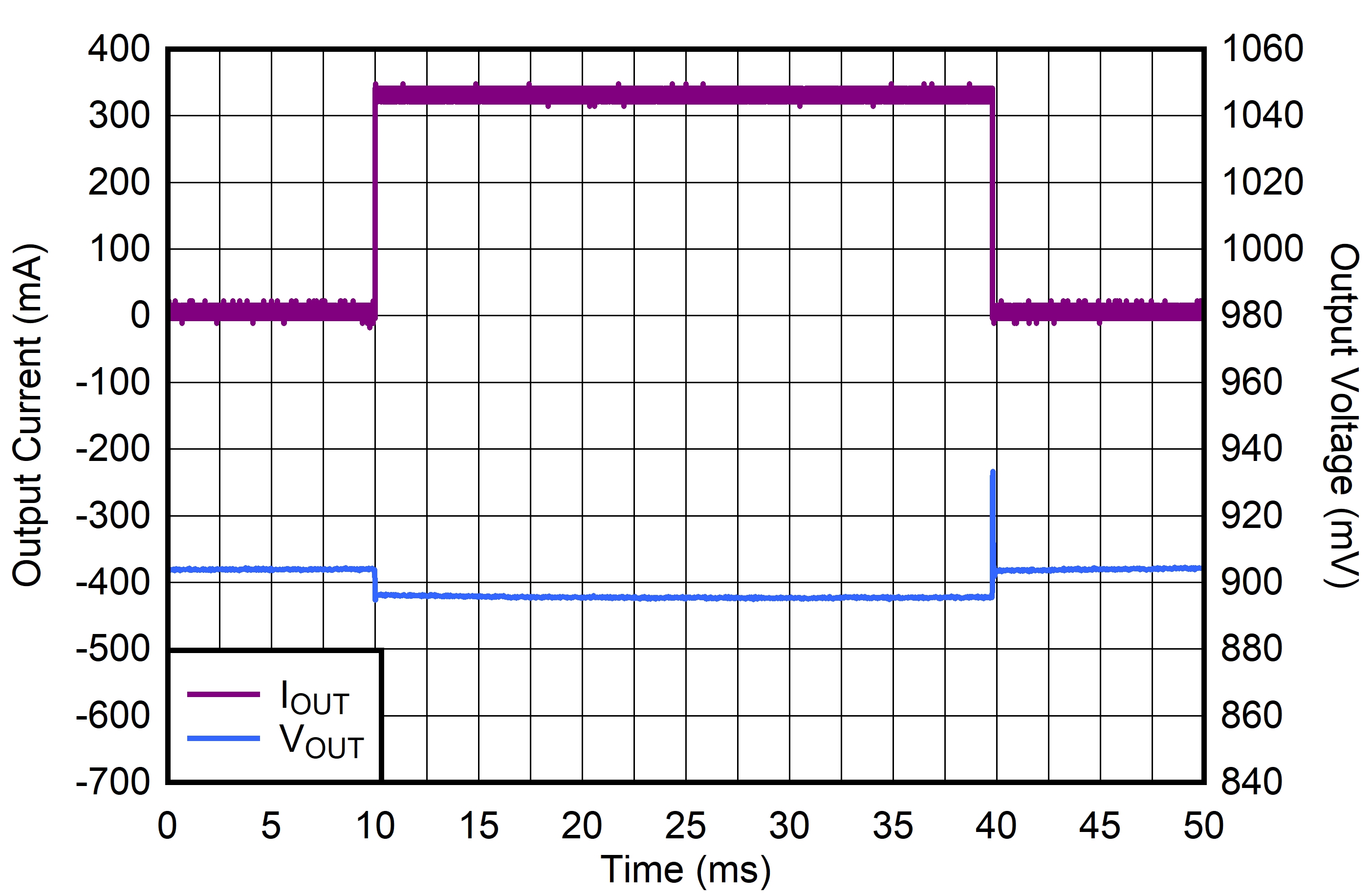
GUID-20211210-SS0I-PD2W-GSK0-5NRLTCLRGDXJ-low.jpg
tr = tf = 1 μs
Figure 6-20 Load Transient From 100 μA to 320 mA
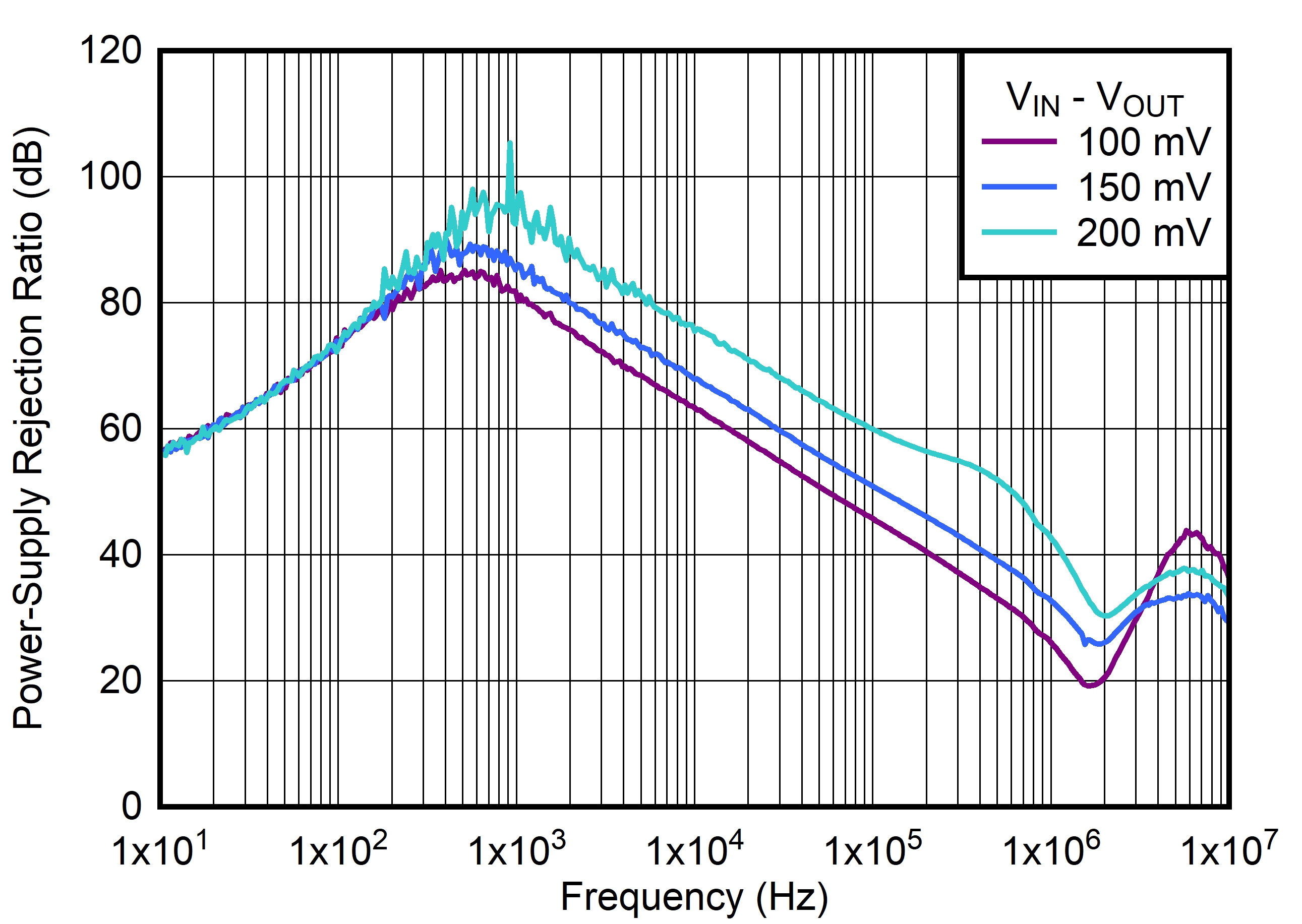
GUID-20211210-SS0I-FZWP-PGJ5-LQTBCRPXWZFB-low.jpg
CBIAS = 0 μF, IOUT = 300 mA
Figure 6-22 VIN PSRR vs Frequency and VIN – VOUT
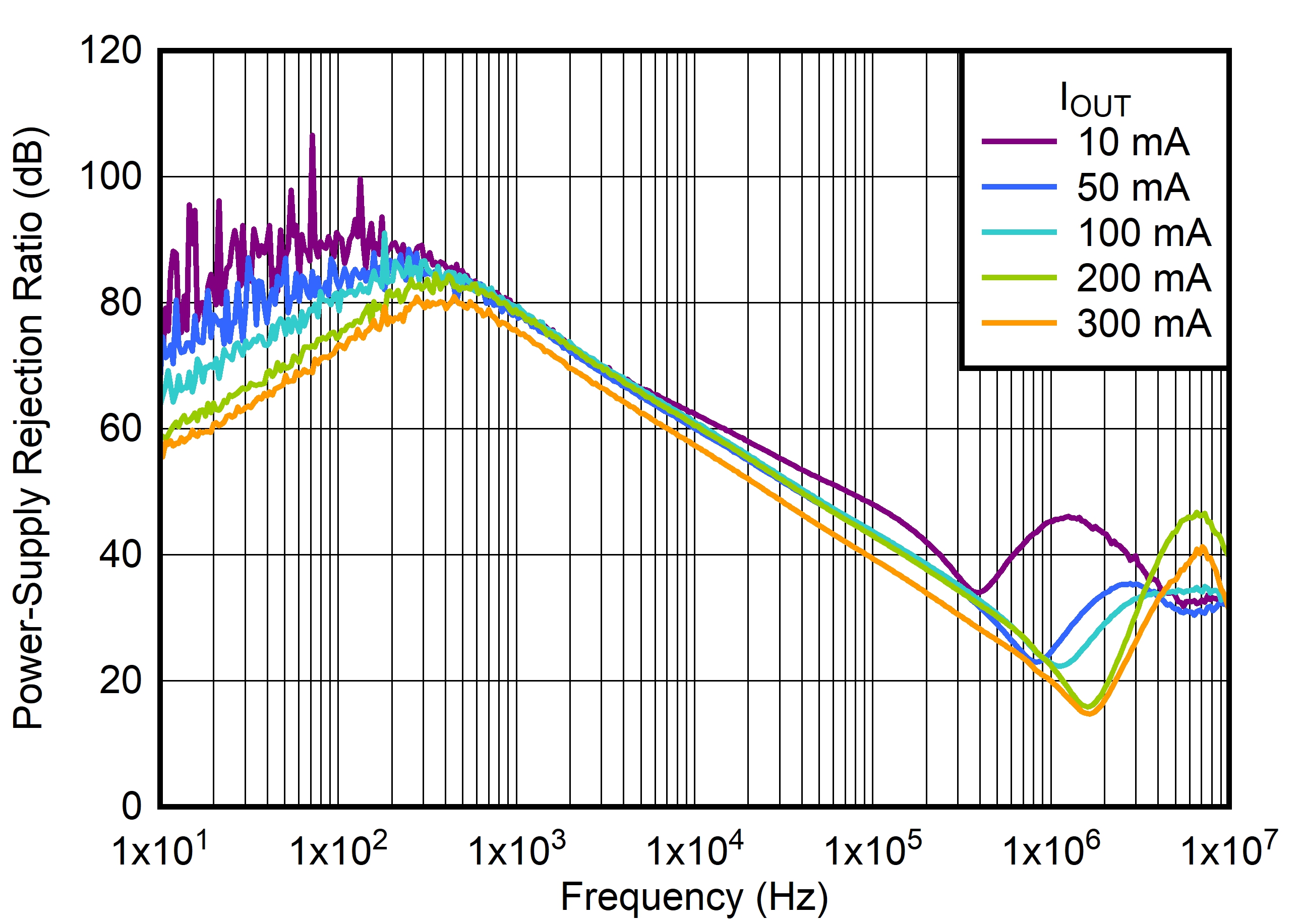
GUID-20211210-SS0I-6LPL-0W9T-PHC8WLM889LJ-low.jpg
CBIAS = 0 μF
Figure 6-24 VIN PSRR vs Frequency and IOUT
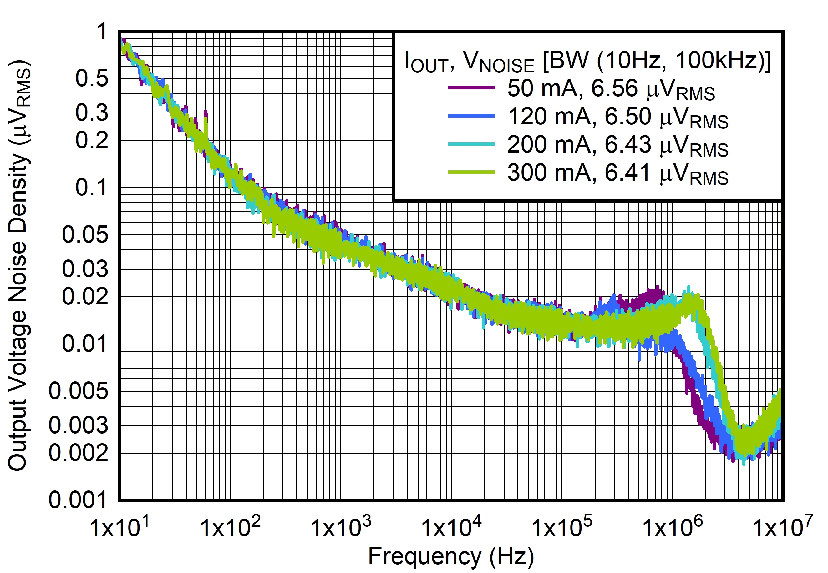
GUID-20211210-SS0I-C1N9-7S8W-63B7TLBXK4GB-low.jpg
 
Figure 6-26 Output Noise vs Frequency and IOUT