SBVS372C December 2018 – December 2022 TPS7A25
PRODUCTION DATA
- 1 Features
- 2 Applications
- 3 Description
- 4 Revision History
- 5 Pin Configuration and Functions
- 6 Specifications
- 7 Typical Characteristics
-
8 Detailed Description
- 8.1 Overview
- 8.2 Functional Block Diagrams
- 8.3 Feature Description
- 8.4 Device Functional Modes
- 9 Device and Documentation Support
- 10Mechanical, Packaging, and Orderable Information
Package Options
Refer to the PDF data sheet for device specific package drawings
Mechanical Data (Package|Pins)
- DRV|6
Thermal pad, mechanical data (Package|Pins)
- DRV|6
Orderable Information
3 Description
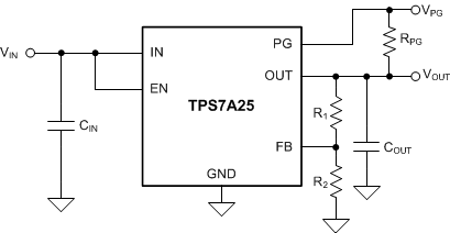
The TPS7A25 low-dropout (LDO) linear voltage regulator introduces a combination of a 2.4-V to 18-V input voltage range with very-low quiescent current (IQ). These features help modern appliances meet increasingly stringent energy requirements, and help extend battery life in portable-power solutions.
The TPS7A25 is available in both fixed and adjustable versions. For more flexibility or higher output voltages, the adjustable version uses feedback resistors to set the output voltage from 1.24 V to 17.64 V. Both versions have a 1% output regulation accuracy that provides precision regulation for most microcontroller (MCU) references.
The TPS7A25 LDO operates more efficiently than standard linear regulators because the maximum dropout voltage is less than 340 mV at 300 mA of current. This maximum dropout voltage allows for 92.5% efficiency from a 5.4-V input voltage (VIN) to a 5.0-V output voltage (VOUT).
The power-good (PG) indicator can be used to either hold an MCU in reset until power is good, or for sequencing. The PG pin is an open-drain output; therefore, the pin is easily level-shifted for monitoring by a rail other than VOUT. The built-in current limit and thermal shutdown help protect the regulator in the event of a load short or fault.
For a higher output current alternative, consider the TPS7A26.
| PART NUMBER | PACKAGE | BODY SIZE (NOM) |
|---|---|---|
| TPS7A25 | DRV (WSON, 6) | 2.00 mm × 2.00 mm |
 Typical Application
Circuit