SBVS226 August 2015 TPS7A4001-EP
PRODUCTION DATA.
- 1 Features
- 2 Applications
- 3 Description
- 4 Revision History
- 5 Pin Configuration and Functions
- 6 Specifications
- 7 Detailed Description
- 8 Application and Implementation
- 9 Power Supply Recommendations
- 10Layout
- 11Device and Documentation Support
- 12Mechanical, Packaging, and Orderable Information
Package Options
Mechanical Data (Package|Pins)
- DGN|8
Thermal pad, mechanical data (Package|Pins)
- DGN|8
Orderable Information
1 Features
- Very High Maximum Input Voltage: 100 V
- Wide Input Voltage Range: 7 to 100 V
- Accuracy:
- Nominal: 1%
- Over Line, Load, and Temperature: 2.7%
- Low Quiescent Current: 25 µA
- Quiescent Current at Shutdown: 4.1 µA
- Maximum Output Current: 50 mA
- CMOS Logic-Level-Compatible Enable Pin
- Adjustable Output Voltage from about 1.175 to
90 V - Stable With Ceramic Capacitors:
- Input Capacitance: ≥1 µF
- Output Capacitance: ≥4.7 µF
- Dropout Voltage: 290 mV
- Built-In Current Limit and Thermal Shutdown Protection
- Package: High Thermal Performance HVSSOP PowerPAD™
-
Supports Defense, Aerospace, and Medical Applications
- Controlled Baseline
- One Assembly and Test Site
- One Fabrication Site
- Available in Military (–55°C to 125°C) Temperature Range
- Extended Product Life Cycle
- Extended Product-Change Notification
- Product Traceability
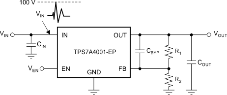
Typical Application Schematic

2 Applications
- Microprocessors, Microcontrollers Powered by Industrial Busses With High Voltage Transients
- Industrial Automation
- Telecom Infrastructure
- Automotive
- Power over Ethernet (PoE)
- LED Lighting
- Bias Power Supplies
3 Description
The TPS7A4001-EP device is a very high voltage-tolerant linear regulator that offers the benefits of a thermally-enhanced package (HVSSOP) and is able to withstand continuous DC or transient input voltages of up to 100 V.
The TPS7A4001-EP device is stable with any output capacitance greater than 4.7 µF and any input capacitance greater than 1 µF (over temperature and tolerance). Therefore, implementations of this device require minimal board space because of its miniaturized packaging (HVSSOP) and a potentially small output capacitor. In addition, the TPS7A4001-EP device offers an enable pin (EN) compatible with standard CMOS logic to enable a low-current shutdown mode.
The TPS7A4001-EP device has an internal thermal shutdown and current limiting to protect the system during fault conditions. The TPS7A4001-EP device has an operating temperature range of TJ = –55°C to 125°C.
In addition, the TPS7A4001-EP device is ideal for generating a low-voltage supply from intermediate voltage rails in telecom and industrial applications; not only can it supply a well-regulated voltage rail, but it can also withstand and maintain regulation during very high and fast voltage transients. These features translate to simpler and more cost-effective electrical surge-protection circuitry for a wide range of applications, including PoE, bias supply, and LED lighting.
Device Information(1)
| PART NUMBER | PACKAGE | BODY SIZE (NOM) |
|---|---|---|
| TPS7A4001-EP | HVSSOP (8) | 3.00 mm × 5.00 mm |
- For all available packages, see the orderable addendum at the end of the data sheet.
4 Revision History
| DATE | REVISION | NOTES |
|---|---|---|
| August 2015 | * | Initial release. |