SBVS204F June 2012 – September 2014
PRODUCTION DATA.
- 1 Features
- 2 Applications
- 3 Description
- 4 Revision History
- 5 Pin Configuration and Functions
- 6 Specifications
- 7 Detailed Description
- 8 Application and Implementation
- 9 Power Supply Recommendations
- 10Layout
- 11Device and Documentation Support
- 12Mechanical, Packaging, and Orderable Information
Package Options
Mechanical Data (Package|Pins)
- RGW|20
Thermal pad, mechanical data (Package|Pins)
- RGW|20
Orderable Information
5 Pin Configuration and Functions
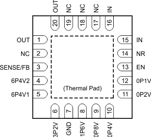
Pin Functions
| PIN | I/O | DESCRIPTION | |
|---|---|---|---|
| NAME | NO. | ||
| 0P1V | 12 | I | When connected to GND, this pin adds 0.1 V to the nominal output voltage of the regulator. |
| Do not connect any voltage other than GND to this pin. If not used, leave this pin floating. | |||
| 0P2V | 11 | I | When connected to GND, this pin adds 0.2 V to the nominal output voltage of the regulator. |
| Do not connect any voltage other than GND to this pin. If not used, leave this pin floating. | |||
| 0P4V | 10 | I | When connected to GND, this pin adds 0.4 V to the nominal output voltage of the regulator. |
| Do not connect any voltage other than GND to this pin. If not used, leave this pin floating. | |||
| 0P8V | 9 | I | When connected to GND, this pin adds 0.8 V to the nominal output voltage of the regulator. |
| Do not connect any voltage other than GND to this pin. If not used, leave this pin floating. | |||
| 1P6V | 8 | I | When connected to GND, this pin adds 1.6 V to the nominal output voltage of the regulator. |
| Do not connect any voltage other than GND to this pin. If not used, leave this pin floating. | |||
| 3P2V | 6 | I | When connected to GND, this pin adds 3.2 V to the nominal output voltage of the regulator. |
| Do not connect any voltage other than GND to this pin. If not used, leave this pin floating. | |||
| 6P4V1 | 5 | I | When connected to GND, this pin adds 6.4 V to the nominal output voltage of the regulator. |
| Do not connect any voltage other than GND to this pin. If not used, leave this pin floating. | |||
| 6P4V2 | 4 | I | When connected to GND, this pin adds 6.4 V to the nominal output voltage of the regulator. |
| Do not connect any voltage other than GND to this pin. If not used, leave this pin floating. | |||
| EN | 13 | I | Enable pin. The device is enabled when the voltage on this pin exceeds the maximum enable voltage, VEN(HI). If enable is not required, tie EN to IN. |
| GND | 7 | — | Ground |
| IN | 15, 16 | I | Input supply. A capacitor greater than or equal to 1 µF must be tied from this pin to ground to assure stability. A 10-µF capacitor is recommended to be connected from IN to GND (as close to the device as possible) to reduce circuit sensitivity to printed circuit board (PCB) layout, especially when long input traces or high source impedances are encountered. |
| NC | 2, 17-19 | — | This pin can be left open or tied to any voltage between GND and IN. |
| NR | 14 | — | Noise reduction pin. When a capacitor is connected from this pin to GND, RMS noise can be reduced to very low levels. A capacitor greater than or equal to 10 nF must be tied from this pin to ground to assure stability. A 1-µF capacitor is recommended to be connected from NR to GND (as close to the device as possible) to maximize ac performance and minimize noise. |
| OUT | 1, 20 | O | Regulator output. A capacitor greater than or equal to 10 µF must be tied from this pin to ground to assure stability. A 47-µF ceramic output capacitor is highly recommended to be connected from OUT to GND (as close to the device as possible) to maximize ac performance. |
| SENSE/FB | 3 | I | Control-loop error amplifier input (TPS7A4701 only). |
| This is the SENSE pin if the device output voltage is programmed using ANY-OUT (no external feedback resistors). This pin must be connected to OUT. Connect this pin to the point of load to maximize accuracy. | |||
| This is the FB pin if the device output voltage is set using external resistors. See the Adjustable Operation section for more details. | |||
| SENSE | 3 | I | Control-loop error amplifier input (TPS7A4700 only). |
| This is the SENSE pin of the device and must be connected to OUT. Connect this pin to the point of load to maximize accuracy. | |||
| Thermal Pad | — | Connect the thermal pad to a large-area ground plane. The thermal pad is internally connected to GND. | |