SBVS121E August 2010 – May 2015 TPS7A49
PRODUCTION DATA.
- 1 Features
- 2 Applications
- 3 Description
- 4 Revision History
- 5 Pin Configuration and Functions
- 6 Specifications
- 7 Parameter Measurement Information
- 8 Detailed Description
-
9 Application and Implementation
- 9.1
Application Information
- 9.1.1 Adjustable Operation
- 9.1.2 Capacitor Recommendations
- 9.1.3 Input and Output Capacitor Requirements
- 9.1.4 Noise-Reduction and Feed-Forward Capacitor Requirements
- 9.1.5 Maximum AC Performance
- 9.1.6 Output Noise
- 9.1.7 Post DC-DC Converter Filtering
- 9.1.8 Power-Supply Rejection
- 9.1.9 Transient Response
- 9.1.10 Audio Applications
- 9.1.11 Power for Precision Analog
- 9.2 Typical Application
- 9.3 Do's and Don’ts
- 9.1
Application Information
- 10Power Supply Recommendations
- 11Layout
- 12Device and Documentation Support
- 13Mechanical, Packaging, and Orderable Information
Package Options
Mechanical Data (Package|Pins)
Thermal pad, mechanical data (Package|Pins)
Orderable Information
9 Application and Implementation
NOTE
Information in the following applications sections is not part of the TI component specification, and TI does not warrant its accuracy or completeness. TI’s customers are responsible for determining suitability of components for their purposes. Customers should validate and test their design implementation to confirm system functionality.
9.1 Application Information
The TPS7A49 devices belongs to a family of linear regulators that use an innovative bipolar process to achieve ultralow-noise and very high PSRR levels at a wide input voltage range. These features, combined with a high thermal-performance HVSSOP-8 with a PowerPAD package make this device ideal for high-performance analog applications.
9.1.1 Adjustable Operation
The TPS7A4901 device has an output voltage range of VFB(nom) to 33 V. The nominal output voltage of the device is set by two external resistors; see Figure 29.
R1 and R2 can be calculated for any output voltage range using the formula shown in Equation 2. To ensure stability under no-load conditions, this resistive network must provide a current greater than or equal to 5 μA.
If greater voltage accuracy is required, take into account the output voltage offset contributions resulting from the feedback pin current and use 0.1% tolerance resistors.
9.1.2 Capacitor Recommendations
Use low-equivalent series resistance (ESR) capacitors for the input, output, noise reduction, and bypass capacitors. Ceramic capacitors with X7R and X5R dielectrics are preferred. These dielectrics offer more stable characteristics. Ceramic X7R capacitors offer improved overtemperature performance, whereas ceramic X5R capacitors are more cost-effective and are available in higher values.
High ESR capacitors can degrade PSRR. To ensure stability, maximum ESR must be less than 200 mΩ.
9.1.3 Input and Output Capacitor Requirements
The TPS7A49 family of positive, high-voltage linear regulators achieve stability with a minimum input and output capacitance of 2.2 μF; however, TI highly recommends using a 10-μF capacitor to maximize ac performance. Place the input and output capacitors as close to the pin as possible, on the same side as the device; do not use vias between the capacitor and the pin.
9.1.4 Noise-Reduction and Feed-Forward Capacitor Requirements
Although noise-reduction and feed-forward capacitors (CNR/SS and CFF, respectively) are not needed to achieve stability, TI highly recommends using 10-nF capacitors to minimize noise and maximize ac performance. CNR/SS is a noise-reduction capacitor because it filters out noise from the band gap. For more information on CFF, refer to application report, Pros and Cons of Using a Feedforward Capacitor with a Low-Dropout Regulator (SBVA042). This application report explains the advantages of using CFF (also known as CBYP), and the problems that can occur when using this capacitor.
9.1.5 Maximum AC Performance
To maximize noise and PSRR performance, TI recommends including 10 μF or higher input and output capacitors, and 10-nF noise-reduction and bypass capacitors; see Figure 29. The solution illustrated in Figure 29 delivers minimum noise levels of 15.4 μVRMS and power-supply rejection levels above 52 dB from 10 Hz to 400 kHz; see Figure 18 and Figure 25.
9.1.6 Output Noise
The TPS7A49 provides low output noise when a noise reduction capacitor (CNR/SS) is used.
The noise-reduction capacitor serves as a filter for the internal reference. By using a 10-nF noise reduction capacitor, the output noise is reduced by approximately 75% (from 69 μVRMS to 17 μVRMS); see Figure 26.
The low output voltage noise of the TPS7A49 makes the device an ideal solution for powering noise-sensitive circuitry.
9.1.7 Post DC-DC Converter Filtering
Most of the time, the voltage rails available in a system do not match the voltage requirements for the system. These rails must be stepped up or down, depending on specific voltage requirements.
DC-DC converters are the preferred solution to step up or down a voltage rail when current consumption is not negligible. These converters offer high efficiency with minimum heat generation, but have one primary disadvantage: these converters introduce a high-frequency component (and the associated harmonics) in addition to the dc output signal.
If not filtered properly, this high-frequency component degrades analog circuitry performance, reducing overall system accuracy and precision.
The TPS7A49 offers a wide-bandwidth, very-high power-supply rejection ratio. This specification makes the device ideal for post dc-dc converter filtering, as shown in Figure 28. TI highly recommends using the maximum performance schematic illustrated in Figure 29. Also, verify that the fundamental frequency (and its first harmonic, if possible) is within the bandwidth of the regulator PSRR; see Figure 18.
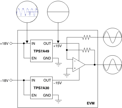 Figure 28. Post DC-DC Converter Regulation to High-Performance Analog Circuitry
9.1.8 Power-Supply Rejection
The 10-nF noise-reduction capacitor greatly improves the TPS7A49 power-supply rejection, achieving up to 15 dB of additional power-supply rejection for frequencies between 110 Hz and 200 kHz.
Additionally, ac performance can be maximized by adding a 10-nF bypass capacitor (CFF) from the FB pin to the OUT pin. This capacitor greatly improves power-supply rejection at lower frequencies for the band from 10 Hz to 200 kHz; see Figure 18.
The very high power-supply rejection of the TPS7A49 makes the device a good choice for powering high-performance analog circuitry, such as operational amplifiers, ADCs, DACS, and audio amplifiers.
9.1.9 Transient Response
As with any regulator, increasing the size of the output capacitor reduces over- and undershoot magnitude, but increases the duration of the transient response.
9.1.10 Audio Applications
Audio applications are extremely sensitive to any distortion and noise in the audio band from 20 Hz to 20 kHz. This stringent requirement demands clean voltage rails to power critical high-performance audio systems.
The very high power-supply rejection ratio (> 55 dB) and low noise at the audio band of the TPS7A49 maximize device performance for audio applications; see Figure 18.
9.1.11 Power for Precision Analog
One of the primary TPS7A49 applications is to provide ultralow-noise voltage rails to high-performance analog circuitry to maximize system accuracy and precision.
The TPS7A49 family of positive high-voltage linear regulators, in conjunction with its negative counterpart (the TPS7A30xx family of negative high-voltage linear regulators), provides ultralow noise, and positive and negative voltage rails for high-performance analog circuitry (such as operational amplifiers, ADCs, DACs, and audio amplifiers).
Because of the ultralow noise levels at high voltages, analog circuitry with high-voltage input supplies can be used. This characteristic allows for high-performance analog solutions to optimize the voltage range and maximize system accuracy.
9.2 Typical Application
9.2.1 Design Requirements
The maximum design goals are as follows:
- VIN = 3 V
- VOUT = 1.2 V
- IOUT = 150 mA
The design optimizes transient response and meets a start-up time of 14 ms with a start-up dominated by the soft-start feature. The input supply comes from a supply on the same printed circuit board (PCB). The design circuit is shown in Figure 29.
The design space consists of CIN, COUT, CNR/SS, R1, and R2, at TA(max) = 75°C.
9.2.2 Detailed Design Procedure
The first step when designing with a linear regulator is to examine the maximum load current, along with the input and output voltage requirements, to determine if the device thermal and dropout voltage requirements can be met. At 150 mA, the input dropout voltage of the TPS7A49 family is a maximum of 600 mV over temperature; therefore, the dropout headroom of 1.8 V is sufficient for operation over both input and output voltage accuracy. Dropout headroom is calculated as VIN – VOUT – VDO(max), and for optimal performance must be at least 1 V. VDO(max) is the maximum dropout allowed, given worst-case load conditions.
The maximum power dissipated in the linear regulator is the maximum voltage dropped across the pass element from the input to the output, multiplied by the maximum load current. In this example, the maximum voltage drop across in the pass element is (3 V – 1.2 V), resulting in VIN – VOUT = 1.8 V. The power dissipated in the pass element is calculated by taking this voltage drop multiplied by the maximum load current. For this example, the maximum power dissipated in the linear regulator is 0.2724 W, and is calculated as Equation 3:
where
When the power dissipated in the linear regulator is known, the corresponding junction temperature rise can be calculated. To calculate the junction temperature rise above ambient, the power dissipated must be multiplied by the junction-to-ambient thermal resistance. This calculation gives the worst-case junction temperature; good thermal design can significantly reduce this number. For thermal resistance information, refer to the Power Dissipation section. For this example, using the DGN package, the maximum junction temperature rise is calculated to be 17.3°C. The maximum junction temperature rise is calculated by adding the junction temperature rise to the maximum ambient temperature, which is 75°C for this example. For this example, calculate the maximum junction temperature to be 103.8°C. Keep in mind that the maximum junction temperate must be below 92.3°C for reliable device operation. Additional ground planes, added thermal vias, and air flow all help to lower the maximum junction temperature.
Use the following guidelines to select the values for the remaining components:
To ensure stability under no-load conditions, the current through the resistor network must be greater than 5 µA, as shown in Equation 4:

Next, set the value of R2 to 100 kΩ for a standard 1% value resistor and use Equation 5 to calculate the value of R1.

For R1, select a standard, 1%, 68.1-kΩ resistor.
Use Equation 6 to calculate the start-up time, tSS.

For the soft-start to dominate the start-up conditions, place the start-up time as a result of the current limit at two decades below the soft-start time (at 140 µs). COUT must be at least 2.2 µF for stability, as shown in Equation 7 and Equation 8:


For CIN, assume that the 3-V supply has some inductance, and is placed several inches away from the PCB. For this case, select a 2.2-µF ceramic input capacitor to ensure that the input impedance is negligible to the LDO control loop and to keep the physical size and cost of the capacitor low; this component is a common-value capacitor.
For better PSRR for this design, use a 10-µF input and output capacitor. To reduce the peaks from transients but slow down the recovery time, increase the output capacitor size or add additional output capacitors.
9.2.3 Application Curves
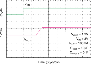 Figure 30. Capacitor-Programmable Soft-Start
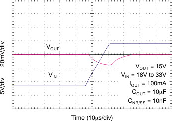 Figure 32. Line Transient Response
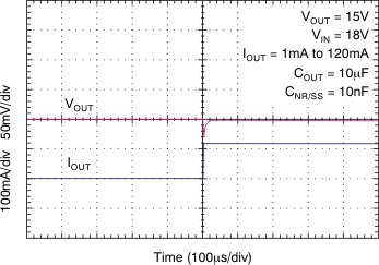 Figure 34. Load Transient Response
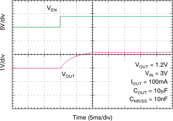 Figure 31. Capacitor-Programmable Soft-Start
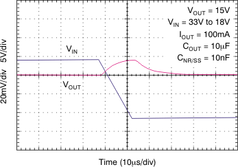 Figure 33. Line Transient Response
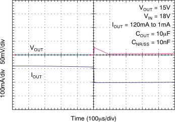 Figure 35. Load Transient Response
9.3 Do's and Don’ts
Place at least one low-ESR, 2.2-µF capacitor as close as possible to both the IN and OUT pins of the regulator to the GND pin.
Provide adequate thermal paths away from the device.
Do not place the input or output capacitor more than 10 mm away from the regulator.
Do not exceed the absolute maximum ratings.
Do not float the enable (EN) pin.
Do not resistively or inductively load the NR/SS pin.

