SBVS311A November 2019 – March 2020 TPS7A54
PRODUCTION DATA.
- 1 Features
- 2 Applications
- 3 Description
- 4 Revision History
- 5 Pin Configuration and Functions
- 6 Specifications
- 7 Detailed Description
-
8 Application and Implementation
- 8.1
Application Information
- 8.1.1 Recommended Capacitor Types
- 8.1.2 Soft Start and Inrush Current
- 8.1.3 Optimizing Noise and PSRR
- 8.1.4 Charge Pump Noise
- 8.1.5 Current Sharing
- 8.1.6 Adjustable Operation
- 8.1.7 Power-Good Operation
- 8.1.8 Undervoltage Lockout (UVLO) Operation
- 8.1.9 Dropout Voltage (VDO)
- 8.1.10 Device Behavior During Transition From Dropout Into Regulation
- 8.1.11 Load Transient Response
- 8.1.12 Reverse Current Protection Considerations
- 8.1.13 Power Dissipation (PD)
- 8.1.14 Estimating Junction Temperature
- 8.1.15 TPS7A54EVM Thermal Analysis
- 8.2 Typical Application
- 8.1
Application Information
- 9 Power Supply Recommendations
- 10Layout
- 11Device and Documentation Support
- 12Mechanical, Packaging, and Orderable Information
Package Options
Mechanical Data (Package|Pins)
- RPS|12
Thermal pad, mechanical data (Package|Pins)
Orderable Information
8.1.6 Adjustable Operation
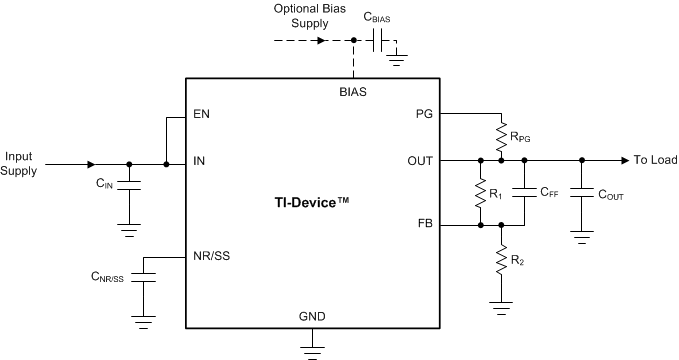
As shown in Figure 44, the output voltage of the TPS7A54 is set using external resistors.
 Figure 44. Typical Circuit
 Use Equation 4 to calculate R1 and R2. This resistive network must provide a current equal to or greater than 5 µA for dc accuracy. To optimize the noise and PSRR, use an R1 of 12.1 kΩ.
Equation 4. VOUT = VNR/SS × (1 + R1 / R2)
Table 5 shows the resistor combinations required to achieve several common rails using standard 1%-tolerance resistors.
Table 5. Recommended Feedback-Resistor Values
| TARGETED OUTPUT VOLTAGE
(V) |
FEEDBACK RESISTOR VALUES(1) | CALCULATED OUTPUT VOLTAGE
(V) |
|
|---|---|---|---|
| R1 (kΩ) | R2 (kΩ) | ||
| 0.9 | 12.4 | 100 | 0.899 |
| 0.95 | 12.4 | 66.5 | 0.949 |
| 1.00 | 12.4 | 49.9 | 0.999 |
| 1.10 | 12.4 | 33.2 | 1.099 |
| 1.20 | 12.4 | 24.9 | 1.198 |
| 1.50 | 12.4 | 14.3 | 1.494 |
| 1.80 | 12.4 | 10 | 1.798 |
| 1.90 | 12.1 | 8.87 | 1.89 |
| 2.50 | 12.4 | 5.9 | 2.48 |
| 2.85 | 12.1 | 4.75 | 2.838 |
| 3.00 | 12.1 | 4.42 | 2.990 |
| 3.30 | 11.8 | 3.74 | 3.324 |
| 3.60 | 12.1 | 3.48 | 3.582 |
| 4.5 | 11.8 | 2.55 | 4.502 |
| 5.00 | 12.4 | 2.37 | 4.985 |
(1) R1 is connected from OUT to FB; R2 is connected from FB to GND.