SBVS395 July 2022 TPS7A57
PRODUCTION DATA
- 1 Features
- 2 Applications
- 3 Description
- 4 Revision History
- 5 Pin Configuration and Functions
- 6 Specifications
-
7 Detailed Description
- 7.1 Overview
- 7.2 Functional Block Diagram
- 7.3
Feature Description
- 7.3.1 Output Voltage Setting and Regulation
- 7.3.2 Low-Noise, Ultra-High Power-Supply Rejection Ratio (PSRR)
- 7.3.3 Programmable Soft-Start (NR/SS Pin)
- 7.3.4 Precision Enable and UVLO
- 7.3.5 Charge Pump Enable and BIAS Rail
- 7.3.6 Power-Good Pin (PG Pin)
- 7.3.7 Active Discharge
- 7.3.8 Thermal Shutdown Protection (TSD)
- 7.4 Device Functional Modes
-
8 Application and Implementation
- 8.1
Application Information
- 8.1.1 Precision Enable (External UVLO)
- 8.1.2 Undervoltage Lockout (UVLO) Operation
- 8.1.3 Dropout Voltage (VDO)
- 8.1.4 Input and Output Capacitor Requirements (CIN and COUT)
- 8.1.5 Recommended Capacitor Types
- 8.1.6 Soft-Start, Noise Reduction (NR/SS Pin), and Power-Good (PG Pin)
- 8.1.7 Optimizing Noise and PSRR
- 8.1.8 Adjustable Operation
- 8.1.9 Load Transient Response
- 8.1.10 Current Limit and Foldback Behavior
- 8.1.11 Charge Pump Operation
- 8.1.12 Sequencing
- 8.1.13 Power-Good Functionality
- 8.1.14 Output Impedance
- 8.1.15 Paralleling for Higher Output Current and Lower Noise
- 8.1.16 Current Mode Margining
- 8.1.17 Voltage Mode Margining
- 8.1.18 Power Dissipation (PD)
- 8.1.19 Estimating Junction Temperature
- 8.1.20 TPS7A57EVM-081 Thermal Analysis
- 8.2 Typical Application
- 8.3 Power Supply Recommendations
- 8.4 Layout
- 8.1
Application Information
- 9 Device and Documentation Support
- 10Mechanical, Packaging, and Orderable Information
Package Options
Mechanical Data (Package|Pins)
- RTE|16
Thermal pad, mechanical data (Package|Pins)
- RTE|16
Orderable Information
8.1.9 Load Transient Response
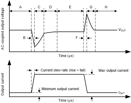
The load-step transient response is the LDO output voltage response to load current, whereby output voltage regulation is maintained. There are two key transitions during a load transient response: the transition from a light to a heavy load, and the transition from a heavy to a light load. The regions shown in Figure 8-9 are broken down in this section. Regions A, E, and H are where the output voltage is in steady-state regulation.
 Figure 8-9 Load
Transient Waveform
Figure 8-9 Load
Transient WaveformDuring transitions from a light load to a heavy load:
- The initial voltage dip is a result of the depletion of the output capacitor charge and parasitic impedance to the output capacitor (region B)
- Recovery from the dip results from the LDO increasing its sourcing current, and leads to output voltage regulation (region C)
During transitions from a heavy load to a light load:
- The initial voltage rise results from the LDO sourcing a large current, and leads to the output capacitor charge to increase (region F)
- Recovery from the rise results from the LDO decreasing its sourcing current in combination with the load discharging the output capacitor (region G)
Transitions between current levels changes the internal power dissipation because the device is a high-current device (region D). The change in power dissipation changes the die temperature during these transitions, and leads to a slightly different voltage level. This temperature-dependent output voltage level shows up in the various load transient responses.
A larger output capacitance reduces the peaks during a load transient but slows down the response time of the device. A larger dc load also reduces the peaks because the amplitude of the transition is lowered and a higher current discharge path is provided for the output capacitor.