SLVSA98F May   2010  – March 2020 TPS7A65-Q1

PRODUCTION DATA.  

  1. Features
  2. Applications
  3. Description
    1.     Device Images
      1.      Typical Application Schematic
      2.      Typical Regulator Stability
  4. Revision History
  5. Pin Configuration and Functions
    1.     Pin Functions
  6. Specifications
    1. 6.1 Absolute Maximum Ratings
    2. 6.2 ESD Ratings
    3. 6.3 Recommended Operating Conditions
    4. 6.4 Thermal Information
    5. 6.5 Electrical Characteristics
    6. 6.6 Dissipation Ratings
    7. 6.7 Typical Characteristics
  7. Detailed Description
    1. 7.1 Overview
    2. 7.2 Functional Block Diagram
    3. 7.3 Feature Description
      1. 7.3.1 Power Up
      2. 7.3.2 Charge-Pump Operation
      3. 7.3.3 Low-Power Mode
      4. 7.3.4 Undervoltage Shutdown
      5. 7.3.5 Low-Voltage Tracking
      6. 7.3.6 Integrated Fault Protection
      7. 7.3.7 Thermal Shutdown
    4. 7.4 Device Functional Modes
      1. 7.4.1 Operation With VIN Lower Than 4 V
      2. 7.4.2 Operation With VIN Larger Than 4 V
  8. Application and Implementation
    1. 8.1 Application Information
    2. 8.2 Typical Application
      1. 8.2.1 Design Requirements
      2. 8.2.2 Detailed Design Procedure
      3. 8.2.3 Application Curve
  9. Power Supply Recommendations
  10. 10Layout
    1. 10.1 Layout Guidelines
      1. 10.1.1 Power Dissipation and Thermal Considerations
    2. 10.2 Layout Example
  11. 11Device and Documentation Support
    1. 11.1 Receiving Notification of Documentation Updates
    2. 11.2 Community Resources
    3. 11.3 Trademarks
    4. 11.4 Electrostatic Discharge Caution
    5. 11.5 Glossary
  12. 12Mechanical, Packaging, and Orderable Information

Package Options

Mechanical Data (Package|Pins)
Thermal pad, mechanical data (Package|Pins)
Orderable Information

Pin Configuration and Functions

KVU Package
3-Pin TO-252
Top View
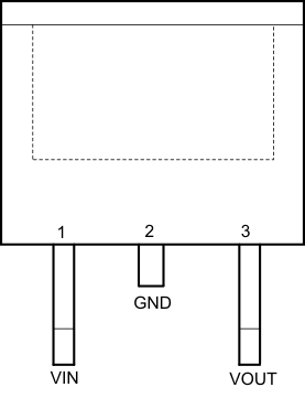
TPS7A65-Q1 pinout_kvu3_lvsa98.gif

Pin Functions

PIN I/O DESCRIPTION
NO. NAME
1 VIN I Input voltage pin: The unregulated input voltage is supplied to this pin. A bypass capacitor is connected between VIN pin and GND pin to dampen input line transients.
2 GND I/O Ground pin: This is signal ground pin of the IC.
3 VOUT O Regulated output voltage pin: This is a regulated voltage output (VOUT = 3.3 V or 5 V, as applicable) pin with a limitation on maximum output current. To achieve stable operation and prevent oscillation, an external output capacitor (COUT) with low ESR is connected between this pin and the GND pin.