SBVS343A March 2019 – September 2019 TPS7A78
PRODUCTION DATA.
- 1 Features
- 2 Applications
- 3 Description
- 4 Revision History
- 5 Pin Configuration and Functions
- 6 Specifications
-
7 Detailed Description
- 7.1 Overview
- 7.2 Functional Block Diagram
- 7.3
Feature Description
- 7.3.1 Active Bridge Control
- 7.3.2 Full-Bridge (FB) and Half-Bridge (HB) Configurations
- 7.3.3 4:1 Switched-Capacitor Voltage Reduction
- 7.3.4 Undervoltage Lockout Circuits (VUVLO_SCIN) and (VUVLO_LDO_IN)
- 7.3.5 Dropout Voltage Regulation
- 7.3.6 Current Limit
- 7.3.7 Programmable Power-Fail Detection
- 7.3.8 Power-Good (PG) Detection
- 7.3.9 Thermal Shutdown
- 7.4 Device Functional Modes
-
8 Application and Implementation
- 8.1
Application Information
- 8.1.1 Recommended Capacitor Types
- 8.1.2 Input and Output Capacitors Requirements
- 8.1.3 Startup Behavior
- 8.1.4 Load Transient
- 8.1.5 Standby Power and Output Efficiency
- 8.1.6 Reverse Current
- 8.1.7 Switched-Capacitor Stage Output Impedance
- 8.1.8 Power Dissipation (PD)
- 8.1.9 Estimating Junction Temperature
- 8.2
Typical Application
- 8.2.1 Design Requirements
- 8.2.2
Detailed Design Procedure
- 8.2.2.1 Calculating the Cap-Drop Capacitor CS
- 8.2.2.2 Calculating the Surge Resistor RS
- 8.2.2.3 Checking for the Device Maximum ISHUNT Current
- 8.2.2.4 Calculating the Bulk Capacitor CSCIN
- 8.2.2.5 Calculating the PFD Pin Resistor Dividers for a Power-Fail Detection
- 8.2.2.6 Summary of the Typical Application Design Components
- 8.2.3 Application Curves
- 8.1
Application Information
- 9 Power Supply Recommendations
- 10Layout
- 11Device and Documentation Support
- 12Mechanical, Packaging, and Orderable Information
Package Options
Mechanical Data (Package|Pins)
- PWP|14
Thermal pad, mechanical data (Package|Pins)
- PWP|14
Orderable Information
7.3.2 Full-Bridge (FB) and Half-Bridge (HB) Configurations
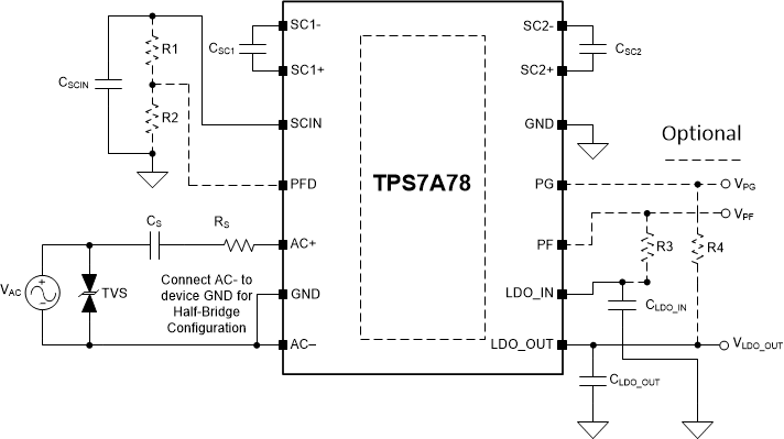
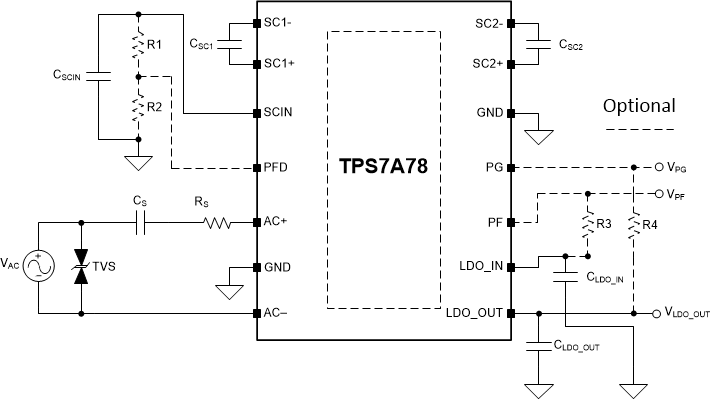
The TPS7A78 can be configured to operate either in full-bridge (FB) or half-bridge (HB) configurations. HB configuration ties the AC input pin without the series CS and RS components to the device GND pins. See Figure 14 and Figure 15 for the HB and FB configurations.
 Figure 14. Typical Schematic Half-Bridge Configuration
  Figure 15. Typical Schematic Full-Bridge Configuration
 NOTE
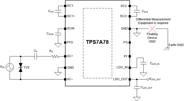
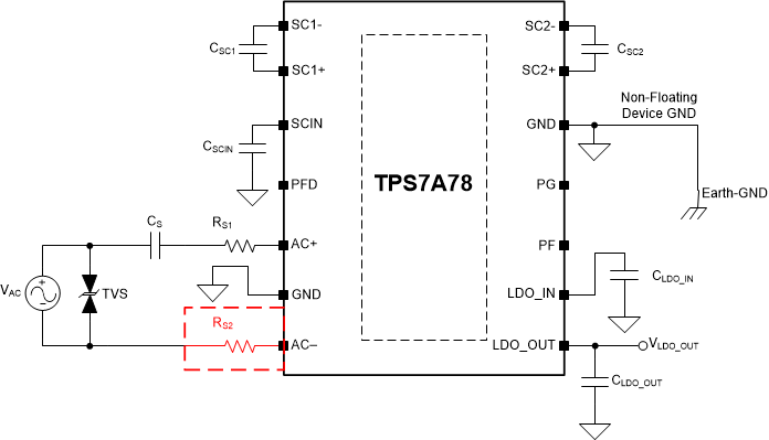
When FB configuration is used, do not tie the device GNDs to earth GND neither schematically nor accidentally via an earth-grounded oscilloscope or measurement equipment because the device GNDs and earth GND are at different voltage potentials. Doing so and can cause damage to the device and external equipment. Tying the device GND pins to earth GND when FB configuration is used is only acceptable if a second surge resistor RS is used on the AC input pin side without the series CS and first RS, as illustrated in Figure 16 with floating device GND pins and Figure 17 with non-floating (earth grounded) device GND pins.
 Figure 16. Full-Bridge Floating Device GND
  Figure 17. Full-Bridge Non-Floating Device GND