SBVS289A August 2017 – September 2017 TPS7A88-Q1
PRODUCTION DATA.
- 1 Features
- 2 Applications
- 3 Description
- 4 Revision History
- 5 Pin Configuration and Functions
- 6 Specifications
- 7 Detailed Description
- 8 Application and Implementation
- 9 Power Supply Recommendations
- 10Layout
- 11Device and Documentation Support
- 12Mechanical, Packaging, and Orderable Information
Package Options
Refer to the PDF data sheet for device specific package drawings
Mechanical Data (Package|Pins)
- RTJ|20
Thermal pad, mechanical data (Package|Pins)
Orderable Information
1 Features
- AEC-Q100 Qualified With the Following Results:
- Temperature Grade 1: –40°C ≤ TA ≤ +125°C
- HBM ESD Classification Level 2
- CDM ESD Classification Level C5
- Two Independent LDO Channels
- Low Output Noise: 4 µVRMS (10 Hz to 100 kHz)
- Low Dropout: 230 mV (Maximum) at 1 A
- Wide Input Voltage Range: 1.4 V to 6.5 V
- Wide Output Voltage Range: 0.8 V to 5.15 V
- High Power-Supply Ripple Rejection:
- 70 dB at 100 Hz
- 40 dB at 100 kHz
- 40 dB at 1 MHz
- 1% Accuracy Over Line, Load, and Temperature
- Excellent Load Transient Response
- Adjustable Start-Up Inrush Control
- Selectable Soft-Start Charging Current
- Independent Open-Drain Power-Good (PG) Outputs
- Stable With a 10-µF or Larger Ceramic Output Capacitor
- Low Thermal Resistance: RθJA = 39.8°C/W
- 4-mm × 4-mm Wettable Flank WQFN Package
2 Applications
- RF and Radar Power in Automotive Applications
- Automotive ADAS ECUs
- Telematic Control Units
- Infotainment and Clusters
- High-Speed I/F (PLL and VCO)
3 Description
The TPS7A88-Q1 is a dual, low-noise (4 µVRMS), low-dropout (LDO) voltage regulator capable of sourcing 1 A per channel with 250 mV of maximum dropout.
The TPS7A88-Q1 provides the flexibility of two independent LDOs and approximately 50% smaller solution size than two single-channel LDOs. Each output is adjustable with external resistors from 0.8 V to 5.15 V. The TPS7A88-Q1 wide input-voltage range supports operation as low as 1.4 V and up to 6.5 V.
With 1% output voltage accuracy (over line, load, and temperature) and soft-start capabilities to reduce in-rush current, the TPS7A88-Q1 is ideal for powering sensitive analog low-voltage devices (such as voltage-controlled oscillators [VCOs], analog-to-digital converters [ADCs], digital-to-analog converters [DACs], high-end processors, and field-programmable gate arrays [FPGAs]).
The TPS7A88-Q1 is designed to power noise-sensitive components such as those found in RF, radar communications, and telematic applications. The low 4-µVRMS output noise and wideband PSRR (40 dB at 1 MHz) minimizes phase noise and clock jitter. These features maximize performance of clocking devices, ADCs, and DACs. The TPS7A88-Q1 features wettable flanks for simple optical inspection.
Device Information(1)
| PART NUMBER | PACKAGE | BODY SIZE (NOM) |
|---|---|---|
| TPS7A88-Q1 | WQFN (20) | 4.00 mm × 4.00 mm |
- For all available packages, see the package option addendum at the end of the data sheet.
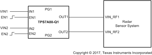
Typical Application Diagram

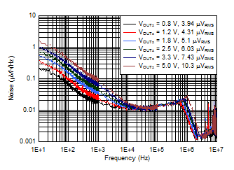
Spectral Noise Density vs Output Voltage
