SLVSCP3C January 2015 – July 2016 TPS7B4253-Q1
PRODUCTION DATA.
- 1 Features
- 2 Applications
- 3 Description
- 4 Revision History
- 5 Pin Configuration and Functions
- 6 Specifications
-
7 Detailed Description
- 7.1 Overview
- 7.2 Functional Block Diagram
- 7.3 Feature Description
- 7.4 Device Functional Modes
- 8 Application and Implementation
- 9 Power Supply Recommendations
- 10Layout
- 11Device and Documentation Support
- 12Mechanical, Packaging, and Orderable Information
Package Options
Mechanical Data (Package|Pins)
Thermal pad, mechanical data (Package|Pins)
Orderable Information
1 Features
- Qualified for Automotive Applications
- AEC-Q100 Qualified With the Following Results:
- Device Temperature Grade 1: –40°C to +125°C Ambient Operating Temperature Range
- Device HBM ESD Classification Level 3A
- Device CDM ESD Classification Level C6
- –40 to 45-V Wide Input-Voltage Range (Maximum)
- Output Voltage Adjusts Down to:
- 1.5 to 40 V (HTSSOP)
- 2 to 40 V (SO PowerPAD™)
- 300-mA Output Current Capability
- Very-Low Output Tracking Tolerance, ±4 mV
- 320-mV Low Dropout Voltage when IOUT = 200 mA
- Separate Pins for Enable and Tracking Inputs (HTSSOP only)
- Low Quiescent Current (IQ):
- < 4 µA when EN = LOW
- 60 µA (Typical) at Light Loads
- Extremely Wide ESR Range.
- Stable With 10- to 500-µF Ceramic Output Capacitor, ESR 1 mΩ to 20 Ω
- Reverse Polarity Protection
- Current-Limit and Thermal-Shutdown Protection
- Output Short-Circuit Proof to Ground and Supply
- Inductive Clamp at OUT Pin
- Available in the Following Packages:
- 8-Pin SO PowerPAD Package
- 20-Pin HTSSOP Package
2 Applications
- Off-Board Sensor Supply
- High-Precision Voltage Tracking
- Power Switch for Off-Board Load
3 Description
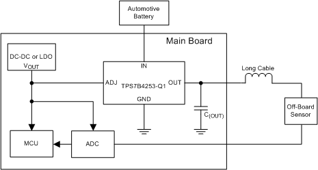
For automotive off-board sensors and small current off-board modules, the power supply is through a long cable from the main board. In such cases, protection is required in the power devices for the off-board loads to prevent the onboard components from damage during a short to GND or short to battery caused by a broken cable. Off-board sensors require consistent power supply as onboard components to secure high accuracy of data acquisition.
The TPS7B4253-Q1 device is designed for automotive applications with a 45-V load dump. The device can either be used as one tracking low-dropout (LDO) regulator or voltage tracker to build one closed power loop for off-board sensors with an onboard main supply. The output of the device is accurately regulated by a reference voltage at the ADJ pin.
To provide an accurate power supply to the off-board modules, the device offers a 4-mV ultralow tracking tolerance between the ADJ and FB pins across temperature. The back-to-back PMOS topology eliminates the need for an external diode under reverse polarity condition. The TPS7B4253-Q1 device also includes thermal shutdown, inductive clamp, overload, and short-to-battery protection to prevent damage to onboard components during extreme conditions.
Device Information(1)
| PART NUMBER | PACKAGE | BODY SIZE (NOM) |
|---|---|---|
| TPS7B4253-Q1 | SO PowerPAD (8) | 4.89 mm × 3.90 mm |
| HTSSOP (20) | 6.50 mm × 4.40 mm |
- For all available packages, see the orderable addendum at the end of the data sheet.
Typical Application Schematic

4 Revision History
Changes from B Revision (January 2016) to C Revision
- Changed the following parameters in the Recommended Operating Conditions table to show values for HTSSOP and SO PowerPAD packages: VADJ, VFB, and VOUT Go
- Corrected the Functional Block DiagramGo
- Added the HTSSOP package as the example for the Application With Output Voltage Equal to the Reference Voltage sectionGo
- Corrected the Output Voltage Equals the Reference Voltage figureGo
- Added the Receiving Notification of Documentation Updates section Go
Changes from A Revision (August 2015) to B Revision
- Changed the note for the reference voltage minus the input voltage parameter in the Absolute Maximum Ratings table Go
- Added values for the SO PowerPAD package for the adjust signal valid parameters in the Electrical Characteristics tableGo
- Changed the test condition for the adjust high signal valid parameter in the Electrical Characteristics tableGo
Changes from * Revision (January 2015) to A Revision
- Changed the device status from Product Preview to Production DataGo