SLVSDU9C February 2017 – December 2022
PRODUCTION DATA
- 1 Features
- 2 Applications
- 3 Description
- 4 Revision History
- 5 Pin Configuration and Functions
- 6 Specifications
-
7 Detailed Description
- 7.1 Overview
- 7.2 Functional Block Diagram
- 7.3
Feature Description
- 7.3.1 Device Enable (EN)
- 7.3.2 Adjustable Power-Good Threshold (PG, PGADJ)
- 7.3.3 Adjustable Power-Good Delay Timer (DELAY)
- 7.3.4 Undervoltage Shutdown
- 7.3.5 Current Limit
- 7.3.6 Thermal Shutdown
- 7.3.7
Integrated Watchdog
- 7.3.7.1 Window Watchdog (WTS, ROSC, FSEL and WRS)
- 7.3.7.2 Standard Watchdog (WTS, ROSC and FSEL)
- 7.3.7.3 Watchdog Service Signal and Watchdog Fault Outputs (WD and WDO)
- 7.3.7.4 ROSC Status Detection (ROSC)
- 7.3.7.5 Watchdog Enable (PG and WD_EN)
- 7.3.7.6 Watchdog Initialization
- 7.3.7.7 Window Watchdog Operation (WTS = Low)
- 7.3.7.8 Standard Watchdog Operation (WTS = High)
- 7.4 Device Functional Modes
- 8 Application and Implementation
- 9 Device and Documentation Support
- 10Mechanical, Packaging, and Orderable Information
Package Options
Mechanical Data (Package|Pins)
- PWP|16
Thermal pad, mechanical data (Package|Pins)
- PWP|16
Orderable Information
7.3.2 Adjustable Power-Good Threshold (PG, PGADJ)
The PG pin is an open-drain output with an external pullup resistor to the regulated supply, and the PGADJ pin is a power-good threshold adjustment pin. Connecting the PGADJ pin to GND sets the power-good threshold value to the default, V(PG_TH). When VOUT exceeds the default power-good threshold, the PG output turns high after the power-good delay period has expired. When VOUT falls below V(PG_TH) – V(PG_HYST), the PG output turns low after a short deglitch time.
The power-good threshold is also adjustable from 1.1 V to 5 V by using an external resistor divider between PGADJ and OUT. The threshold can be calculated using Equation 1:
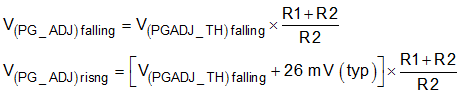
where
- V(PG_ADJ) is the adjustable power-good threshold
- V(PG_REF) is the internal comparator reference voltage of the PGADJ pin, 1.1 V typical, 2% accuracy specified under all conditions
By setting the power-good threshold V(PG_ADJ), when VOUT exceeds this threshold, the PG output turns high after the power-good delay period has expired. When VOUT falls below V(PG_ADJ) – V(PG_HYST), the PG output turns low after a short deglitch time. Figure 7-1 shows typical hardware connections for the PGADJ pin and DELAY pin.
 Figure 7-1 Adjustable Power-Good
Threshold
Figure 7-1 Adjustable Power-Good
Threshold