SLVSD43C May 2015 – February 2019 TPS7B68-Q1
PRODUCTION DATA.
- 1 Features
- 2 Applications
- 3 Description
- 4 Revision History
- 5 Pin Configuration and Functions
- 6 Specifications
-
7 Detailed Description
- 7.1 Overview
- 7.2 Functional Block Diagram
- 7.3
Feature Description
- 7.3.1 Device Enable (EN)
- 7.3.2 Adjustable Power-Good Threshold (PG, PGADJ)
- 7.3.3 Adjustable Power-Good Delay Timer (DELAY)
- 7.3.4 Undervoltage Shutdown
- 7.3.5 Current Limit
- 7.3.6 Thermal Shutdown
- 7.3.7
Integrated Watchdog
- 7.3.7.1 Window Watchdog (WTS, ROSC, FSEL and WRS)
- 7.3.7.2 Standard Watchdog (WTS, ROSC and FSEL)
- 7.3.7.3 Watchdog Service Signal and Watchdog Fault Outputs (WD and WDO)
- 7.3.7.4 ROSC Status Detection (ROSC)
- 7.3.7.5 Watchdog Enable (PG and WD_EN)
- 7.3.7.6 Watchdog Initialization
- 7.3.7.7 Window Watchdog Operation (WTS = Low)
- 7.3.7.8 Standard Watchdog Operation (WTS = High)
- 7.4 Device Functional Modes
- 8 Application and Implementation
- 9 Power Supply Recommendations
- 10Layout
- 11Device and Documentation Support
- 12Mechanical, Packaging, and Orderable Information
Package Options
Mechanical Data (Package|Pins)
- PWP|28
Thermal pad, mechanical data (Package|Pins)
- PWP|28
Orderable Information
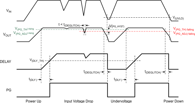
7.3.3 Adjustable Power-Good Delay Timer (DELAY)
The power-good delay period is a function of the value set by an external capacitor on the DELAY pin before turning the PG pin high. Connecting an external capacitor from this pin to GND sets the power-good delay period. The constant current charges an external capacitor until the voltage exceeds a threshold to trip an internal comparator, and Equation 2 determines the power-good delay period:
Equation 2. 

where
- t(DLY) is the adjustable power-good delay period
- CDELAY is the value of the power-good delay capacitor

NOTE:
V(PG_TH) falling = V(PG_TH) rising – V(PG_HYST).If the DELAY pin is open, the default delay time is t(DLY_FIX).