SLVSDQ0K September 2017 – September 2025 TPS7B82-Q1
PRODUCTION DATA
- 1
- 1 Features
- 2 Applications
- 3 Description
- 4 Pin Configuration and Functions
- 5 Specifications
- 6 Detailed Description
- 7 Application and Implementation
- 8 Device and Documentation Support
- 9 Revision History
- 10Mechanical, Packaging, and Orderable Information
Package Options
Mechanical Data (Package|Pins)
Thermal pad, mechanical data (Package|Pins)
Orderable Information
3 Description
In automotive battery-connected applications, low quiescent current (IQ) is important to save power and extend battery lifetime. Ultra-low IQ must be included for always-on systems.
The TPS7B82-Q1 is a low-dropout linear regulator designed to operate with a wide input-voltage range from 3V to 40V (45V load dump protection). Operation down to 3V allows the TPS7B82-Q1 to continue operating during cold-crank and start and stop conditions. With only 2.7µA typical quiescent current at light load, this device is an optimum design for powering microcontrollers (MCUs) and CAN/LIN transceivers in standby systems.
The device features integrated short-circuit and overcurrent protection. This device operates in ambient temperatures from –40°C to +125°C and with junction temperatures from –40°C to +150°C. Additionally, this device uses a thermally conductive package to enable sustained operation despite significant dissipation across the device. Because of these features, the device is designed as a power supply for various automotive applications.
| PART NUMBER | PACKAGE(1) | PACKAGE SIZE(2) |
|---|---|---|
| TPS7B82-Q1 | DGN (HVSSOP, 8) | 3mm × 4.9mm |
| DRV (WSON, 6) | 2mm × 2mm | |
| DRV (WSON wettable flank, 6) | 2mm × 2mm | |
| KVU (TO-252, 5) | 6.6mm × 10.11mm | |
| PWP (HTSSOP, 14) | 5mm × 6.4mm |
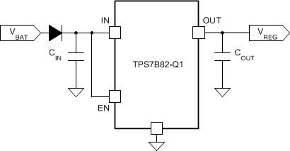
 Typical Application Schematic