SBVS376 November 2020 TPS7B83-Q1
PRODUCTION DATA
- 1 Features
- 2 Applications
- 3 Description
- 4 Revision History
- 5 Pin Configuration and Functions
- 6 Specifications
- 7 Detailed Description
- 8 Application and Implementation
- 9 Power Supply Recommendations
- 10Layout
- 11Device and Documentation Support
- 12Mechanical, Packaging, and Orderable Information
Package Options
Mechanical Data (Package|Pins)
- DCY|4
Thermal pad, mechanical data (Package|Pins)
- DCY|4
Orderable Information
3 Description
The TPS7B83-Q1 is a low-dropout linear
regulator designed to connect to the battery in automotive applications. The device
has an input voltage range extending to 40 V, which allows the device to withstand
transients (such as load dump) that are anticipated in automotive systems. With only
an
18-µA quiescent current, the device is an optimal
solution for powering always-on components such as microcontrollers (MCUs) and
controller area network (CAN) transceivers in standby systems.
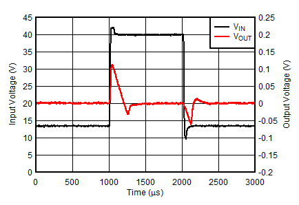
The device has state-of-the-art transient response that allows the output to quickly react to changes in load or line (for example, during cold-crank conditions). Additionally, the device has a novel architecture that minimizes output overshoot when recovering from dropout. During normal operation, the device has a tight DC accuracy of ±1% over line, load, and temperature.
| PART NUMBER | PACKAGE | BODY SIZE (NOM) |
|---|---|---|
| TPS7B83-Q1 | SOT-223 (3) | 6.50 mm × 3.50 mm |
 Typical Application Schematic
 Line Transient Response
 (3-V/µs VIN Slew Rate)