SBVS362D June 2020 – October 2025 TPS7B86-Q1
PRODUCTION DATA
- 1
- 1 Features
- 2 Applications
- 3 Description
- 4 Pin Configuration and Functions
- 5 Specifications
- 6 Detailed Description
-
7 Application and Implementation
- 7.1 Application Information
- 7.2 Typical Application
- 7.3 Power Supply Recommendations
- 7.4 Layout
- 8 Device and Documentation Support
- 9 Revision History
- 10Mechanical, Packaging, and Orderable Information
Package Options
Refer to the PDF data sheet for device specific package drawings
Mechanical Data (Package|Pins)
- DDA|8
- KVU|5
Thermal pad, mechanical data (Package|Pins)
- KVU|5
Orderable Information
4 Pin Configuration and Functions
Figure 4-1 KVU Package,5-Pin TO-252(Top View)
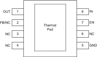
 Figure 4-2 DDA Package (Without PG),
8-Pin HSOIC(Top View)
 Figure 4-3 DDA Package (With PG),
8-Pin HSOIC, B Version(Top View)
Figure 4-4 DDA Package (With PG),
8-Pin HSOIC, D Version(Top View)
8-Pin HSOIC, D Version(Top View)
Table 4-1 Pin Functions
| PIN | TYPE(1) | DESCRIPTION | ||||
|---|---|---|---|---|---|---|
| NAME | NO. | |||||
| KVU | DDA (Without PG) | DDA (B Version) | DDA (D Version) | |||
| DELAY | — | — | 3 | 3 | O | Power-good delay adjustment pin. Connect a capacitor from this pin to GND to set the PG reset delay. Leave this pin floating for a default (t(DLY_FIX)) delay. See the Power-Good (PG) section for more information. If this functionality is not desired, leave this pin floating because connecting this pin to GND causes a permanent increase in the GND current. |
| EN | 2 | 7 | 7 | 6 | I | Enable pin. The device is disabled when the enable pin becomes lower than the enable logic input low level (VIL). Do not leave this pin floating because this pin is high impedance. If left floating, this pin can cause the device to enable or disable. |
| FB/NC | 4 | 2 | 2 | 2 | I | This pin is a feedback pin when using an external resistor divider or an NC pin when using the device with a fixed output voltage. When using the adjustable device, this pin must be connected through a resistor divider to the output for the device to function. If using a fixed output this pin can either be left floating or connected to GND. |
| GND | 3 | 5 | 5 | 4 | G | Ground pin. Connect this pin to the thermal pad with a low-impedance connection. |
| IN | 1 | 8 | 8 | 8 | P | Input power-supply voltage pin. For best transient response and to minimize input impedance, use the recommended value or larger ceramic capacitor from IN to GND as listed in the Recommended Operating Conditions table and the Input Capacitor section. Place the input capacitor as close to the input of the device as possible. |
| NC | — | 3, 4, 6 | 4 | 7 | — | No internal connection. This pin can be left floating or tied to GND for best thermal performance. |
| OUT | 5 | 1 | 1 | 1 | O | Regulated output voltage pin. A capacitor is required from OUT to GND for stability. For best transient response, use the nominal recommended value or larger ceramic capacitor from OUT to GND; see the Recommended Operating Conditions table and the Output Capacitor section. Place the output capacitor as close to output of the device as possible. If using a high equivalent series resistance (ESR) capacitor, decouple the output with a 100nF ceramic capacitor. |
| PG | — | — | 6 | 5 | O | Active-high, power-good pin. An open-drain output indicates when the output voltage reaches VPG(TH,RISING) of the target. Using a feed-forward capacitor can disrupt PG (power good) functionality. See the Power-Good (PG) section for more information. |
| Thermal pad | Pad | Pad | Pad | Pad | — | Thermal pad. Connect the pad to GND for best possible thermal performance. See the Layout section for more information. |
(1) I = input; O = output; P = power; G = ground.