SLVSD81A January 2016 – February 2017 TPS7H1101-SP
PRODUCTION DATA.
- 1 Features
- 2 Applications
- 3 Description
- 4 Revision History
- 5 Description (continued)
- 6 Pin Configuration and Functions
- 7 Specifications
- 8 Detailed Description
- 9 Application and Implementation
- 10Power Supply Recommendations
- 11Layout
- 12Device and Documentation Support
- 13Mechanical, Packaging, and Orderable Information
Package Options
Mechanical Data (Package|Pins)
- HKR|16
Thermal pad, mechanical data (Package|Pins)
Orderable Information
1 Features
-
5962R13202:
- Radiation Hardness Assurance (RHA) up to TID 100 krad (Si)
- Total Ionizing Dose 100 krad (Si)
- ELDRS-Free 100 krad (Si)
- Dose Rate 10 mRAD (si)/s
- Single Event Latchup (SEL) Immune to
LET = 85 MeV-cm2/mg - SEB and SEGR Immune to
LET = 85 MeV-cm2/mg - SET/SEFI Onset Threshold > 40 MeV-cm2/mg, See Radiation Report for Details
- Specifically Designed to Always Upset Low to Avoid Damage to Critical Downstream Component
- SET/SEFI Cross-Section Plot, See Radiation Report for Details
- Ultra-Low VIN Range: 1.5 V to 7 V
- 3-A Maximum Output Current
- Current Share/Parallel Operation to Provide up to 6-A Output Current
- Stable With Ceramic Output Capacitor
- ±2% Accuracy Over Line, Load, and Temperature
- Programmable Soft-Start Through External Capacitor
- Input Enable and Power-Good Output for Power Sequencing
- Ultra-Low Dropout LDO Voltage:
62 mV at 1 A (25°C), VOUT = 1.8 V - Low Noise:
20.33 µVRMS VIN = 2 V, VOUT = 1.8 V at 3 A - PSRR: Over 45 dB at 1 kHz
- Excellent Load/Line Transient Response
- Foldback Current Limit
- See the Tools & Software Tab
- Thermally-Enhanced CFP Package (0.6°C/W RθJC)
2 Applications
- Space Satellite Point of Load Supply for FPGAs, Microcontrollers, ASICs, and Data Converters
- Space Satellite Payloads
- Radiation-Hardened Low-Noise Linear Regulator Power Supply for RF, VCOs, Receivers, and Amplifiers
- Clean Analog Supply Requirements
- Available in Military (–55°C to 125°C) Temperature Range
- Engineering Evaluation (/EM) Samples are Available(1)
3 Description
The TPS7H1101-SP is a radiation-hardened LDO linear regulator that uses a PMOS pass element configuration. This device operates over a wide range of input voltage, from 1.5 V to 7 V while offering excellent PSRR. The TPS7H1101-SP features a precise and programmable foldback current limit implementation with a very-wide adjustment range. To support the complex power requirements of FPGAs, DSPs, or microcontrollers, the TPS7H1101-SP provides enable on and off functionality, programmable SoftStart, current sharing capability, and a PowerGood open-drain output.
Device Information(2)
| PART NUMBER | PACKAGE | BODY SIZE (NOM) |
|---|---|---|
| TPS7H1101-SP | CFP (16) | 11.00 mm × 9.60 mm |
- These units are intended for engineering evaluation only. They are processed to a noncompliant flow (that is, no burn-in, and so forth) and are tested to a temperature rating of 25°C only. These units are not suitable for qualification, production, radiation testing or flight use. Parts are not warranted for performance over the full MIL specified temperature range of –55°C to 125°C or operating life.
- For all available packages, see the orderable addendum at the end of the data sheet.
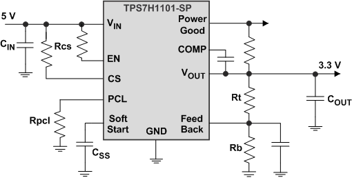
Typical Application Circuit

4 Revision History
Changes from * Revision (January 2016) to A Revision
- Changed accuracy over line, load, and temperature from ±1.25% : to ±2% in the Features sectionGo
- Added I/O values in the Pin Functions tableGo
- Changed COMP pin descriptionGo
- Deleted peak output current spec in Absolute Maximum Ratings tableGo
- Changed max output voltage from VIN : to 7.5 VGo
- Added rise time specification for EN signal in Recommended Operating Conditions tableGo
- Added rise time specification for VIN signal in Recommended Operating Conditions tableGo
- Deleted unnecessary DC input line regulation data in the Electrical Characteristics tableGo
- Deleted worst case dropout voltage specifications Electrical Characteristics tableGo
- Deleted redundant operating junction temperature in the Electrical Characteristics tableGo
- Changed output voltage range from VIN – 0.35 V : to VINGo
- Changed min and typ CSR values from 47500 A/A and 47394 A/A : to 47394 A/A and 47500 A/A, respectively Go
- Added PSRR curve to Typical Characteristics sectionGo
- Changed typo regarding capacitor from CS : to SS in the Soft Start sectionGo
- Added clarification on PG functionality and removed reference to sequencing SS terminal in Power Good (PG) sectionGo
- Deleted description for disable using SS terminal in the Enable/Disable sectionGo
- Changed Stability sectionGo
- Changed Equation 2 (group delay equation)Go
- Added resistor between VIN and EN in Figure 12 as recommendedGo
- Changed values in Table 2 with more accurate output voltagesGo
- Added clarity to current foldback feature in Current Foldback sectionGo
- Changed channel labels to match scope captures in Transient Response sectionGo
- Added parallel operation block diagram to Current Sharing sectionGo
- Added compensation example feedback resistor value (Rbottom) to Compensation sectionGo
- Changed organization of information in Capacitors sectionGo
- Deleted Application CurvesGo
- Added information to Layout Guidelines sectionGo
- Added Receiving Notification of Documentation Updates section to Device and Documentation Support sectionGo