SLVSDW6C April 2017 – April 2021 TPS7H1101A-SP
PRODUCTION DATA
- 1 Features
- 2 Applications
- 3 Description
- 4 Revision History
- 5 Pin Configuration and Functions
- 6 Specifications
- 7 Detailed Description
- 8 Application and Implementation
- 9 Power Supply Recommendations
- 10Layout
- 11Device and Documentation Support
- 12Mechanical, Packaging, and Orderable Information
Package Options
Mechanical Data (Package|Pins)
- HKR|16
- KGD|0
Thermal pad, mechanical data (Package|Pins)
Orderable Information
8.2.1.1 Adjustable Output Voltage (Feedback Circuit)
The output voltage of the TPS7H1101A-SP can be set to a user-programmable level between 0.8 V and 6.65 V. Achieve this by using a resistor divider connected between VOUT, FB, and GND terminals. RTOP connected between VOUT and VFB, and RBOTTOM connected between VFB and GND.
Use Equation 2 to determine VOUT.
Equation 2. 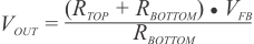
where
- VFB = 0.605 V
Table 8-1 Example Resistor Values for Typical Voltages
| VOUT | Standard 1% Resistors | Standard 0.1% Resistors | ||
|---|---|---|---|---|
| RTOP | RBOTTOM | RTOP | RBOTTOM | |
| 0.8 V | 10.7 kΩ | 33.2 kΩ | 10.7 kΩ | 33.2 kΩ |
| 1 V | 13.7 kΩ | 21 kΩ | 12.6 kΩ | 19.3 kΩ |
| 1.2 V | 11.3 kΩ | 11.5 kΩ | 11.8 kΩ | 12 kΩ |
| 1.5 V | 15.8 kΩ | 10.7 kΩ | 18.2 kΩ | 12.3 kΩ |
| 1.8 V | 23.2 kΩ | 11.8 kΩ | 32 kΩ | 16.2 kΩ |
| 2.5 V | 10.7 kΩ | 3.4 kΩ | 37.9 kΩ | 12.1 kΩ |
| 3.3 V | 51.1 kΩ | 11.5 kΩ | 10.2 kΩ | 2.29 kΩ |
| 4 V | 13.3 kΩ | 2.37 kΩ | 31.2 kΩ | 5.56 kΩ |
| 5 V | 11.5 kΩ | 1.58 kΩ | 16.2 kΩ | 2.23 kΩ |
| 5.5 V | 17.4 kΩ | 2.15 kΩ | 89.8 kΩ | 11.1 kΩ |
| 6 V | 90.9 kΩ | 10.2 kΩ | 10.7 kΩ | 1.2 kΩ |
| 6.5 V | 26.7 kΩ | 2.74 kΩ | 15.2 kΩ | 1.56 kΩ |
| 6.6 V | 11.3 kΩ | 1.15 kΩ | 22.1 kΩ | 2.23 kΩ |
| 6.7 V | 39.2 kΩ | 3.92 kΩ | 13.8 kΩ | 1.37 kΩ |