SLVSDW6C April 2017 – April 2021 TPS7H1101A-SP
PRODUCTION DATA
- 1 Features
- 2 Applications
- 3 Description
- 4 Revision History
- 5 Pin Configuration and Functions
- 6 Specifications
- 7 Detailed Description
- 8 Application and Implementation
- 9 Power Supply Recommendations
- 10Layout
- 11Device and Documentation Support
- 12Mechanical, Packaging, and Orderable Information
Package Options
Mechanical Data (Package|Pins)
- HKR|16
- KGD|0
Thermal pad, mechanical data (Package|Pins)
Orderable Information
8.2.1.3 High-Side Current Sense
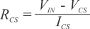
Figure 8-4 shows the cascode NMOS current mirror. VCS must be ≥ 0.3 V for proper biasing. Additionally VCS must be greater than 0.9 · VREF (0.544 V) if foldback current limiting is intended to be enabled. The following example shows the typical calculation of RCS.
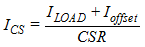
where
- ILOAD is the output load current
- CSR is the current sense ratio
- Ioffset is internal keep-alive bias current times CSR
- Ioffset = 5 µA · CSR
When VIN = 2.3 V, select VCS = 2.05 V, ILOAD = 3 A, CSR = 52000, and Ioffset = 0.26 A, then ICS = 62.69 µA and RCS = 3.99 kΩ.
 Figure 8-4 Cascode NMOS Current Mirror
For TPS7H1101A-SP, Figure 8-5 shows a typical curve VCS vs IOUT for VIN = 2.28 V and RCS = 3.65 kΩ. A resistor connected from the CS terminal to VIN indicates voltage proportional to the output current.
Monitoring current in the CS terminal (ICS vs ILOAD) indicates the current sense ratio between the main PMOSFET and the current sense MOSFET as shown in Figure 8-6. Additionally Figure 8-6 shows the linearity of the CSR ratio across VCS pin voltage range of 0.3 V to VIN. VCS must be ≥ 0.3-V minimum to keep circuit properly biased.
Figure 8-7 shows ILOAD vs ICS across the full range of CSR values.
 vs ILOAD (A)")
| VIN = 2.3 V | VOUT = 1.8 V | y = –0.078x + 2.2853 |
 vs ICS (A)") Figure 8-7 IOUT (A) vs ICS (A)
Figure 8-7 IOUT (A) vs ICS (A) vs ICS (A)")
| VIN = 2.3 V | VOUT = 1.8 V |