SLVSEW6F August 2021 – March 2024 TPS7H2211-SEP , TPS7H2211-SP
PRODUCTION DATA
- 1
- 1 Features
- 2 Applications
- 3 Description
- 4 Device Options
- 5 Related Products
- 6 Pin Configuration and Functions
-
7 Specifications
- 7.1 Absolute Maximum Ratings
- 7.2 ESD Ratings
- 7.3 Recommended Operating Conditions
- 7.4 Thermal Information
- 7.5 Electrical Characteristics: All Devices
- 7.6 Electrical Characteristics: CFP and KGD Options
- 7.7 Electrical Characteristics: HTSSOP Option
- 7.8 Switching Characteristics: All Devices
- 7.9 Quality Conformance Inspection
- 7.10 Typical Characteristics
- 8 Parameter Measurement Information
- 9 Detailed Description
- 10Application and Implementation
- 11Device and Documentation Support
- 12Revision History
- 13Mechanical, Packaging, and Orderable Information
Package Options
Refer to the PDF data sheet for device specific package drawings
Mechanical Data (Package|Pins)
- DAP|32
- KGD|0
- HKR|16
Thermal pad, mechanical data (Package|Pins)
- DAP|32
Orderable Information
9.3.1 Enable and Overvoltage Protection
Figure 9-1 shows how resistor dividers from VIN connected to the EN and OVP pins can be used to set the enable and overvoltage trip points.
 Figure 9-1 Enable and OVP Thresholds Set by
Resistor Dividers
Figure 9-1 Enable and OVP Thresholds Set by
Resistor DividersThe EN pin turns on or turns off the internal switch FETs. An EN voltage greater than VIHEN turns on the switch, and a voltage less than VILEN turns off the switch. The external resistor divider allows the enable threshold to be configured for a different enable rising voltage (VINEN_RISE) and a disable falling voltage (VINEN_FALL) based on the VIHEN and VILEN specifications respectively. Generally, applications are optimized to configure the enable rising voltage. However, if desired the falling voltage can be configured to use the EN pin as an under voltage protection (UVP) feature.
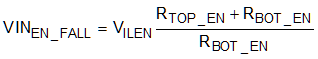
Typically RTOP_EN is set to 100 kΩ and a value for RBOT_EN is calculated. Section 10.2.2.2.2 shows how these resistor values could be calculated. The enable rising and falling threshold parameters are shown in Figure 9-2, and equations to calculate the resulting rising and falling voltages are shown in Equation 1 and Equation 2 respectively. These equations do not take into account the small EN leakage current which has minimal effect on the results.
Additionally, ensure EN is not asserted before VIN is ≥ 75% of its final value as indicated in the electrical characteristics footnote (see Section 7.5). This is only required if VINSR > VOUTSR. This requirement is to prevent a false overcurrent trigger event.
 Figure 9-2 Enable Rising and Falling
Thresholds
Figure 9-2 Enable Rising and Falling
Thresholds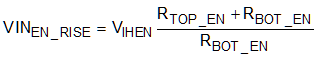
Similarly, the overvoltage protection (OVP) feature can be configured using a resistor divider from VIN connected to the OVP pin. A voltage at the OVP pin greater than VOVPR will turn off the switch FETs, and a voltage less than VOVPF will keep the switch FETs on. If this feature is not desired, the OVP pin must be grounded.
The OVP feature is intended to protect downstream devices from an overvoltage condition (by turning off the eFuse if the OVP threshold is reached). The OVP feature does not protect the TPS7H2211 eFuse itself from higher values of VIN. Follow the 14-V maximum VIN value and the 7-V maximum OVP value in the recommended operating conditions.
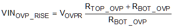
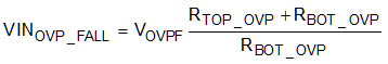
Typically RTOP_OVP is set to 100 kΩ and a value for RBOT_OVP is calculated. Section 10.2.1.2.3 shows how these resistor values could be calculated. The OVP rising and falling threshold parameters are shown in Figure 9-3, and equations to calculate the resulting rising and falling voltages are shown in Equation 3 and Equation 4 respectively. These equations do not take into account the small OVP leakage current which has minimal effect on the results.
 Figure 9-3 OVP Rising and Falling
Thresholds
Figure 9-3 OVP Rising and Falling
Thresholds