SLVSEN7D april 2019 – may 2023 TPS7H4001-SP
PRODMIX
- 1
- 1 Features
- 2 Applications
- 3 Description
- 4 Revision History
- 5 Device Options Table
- 6 Pin Configuration and Functions
-
7 Specifications
- 7.1 Absolute Maximum Ratings
- 7.2 ESD Ratings
- 7.3 Recommended Operating Conditions
- 7.4 Thermal Information
- 7.5 Electrical Characteristics - All Devices
- 7.6 Electrical Characteristics: CDFP and KGD Options
- 7.7 Electrical Characteristics: HTSSOP (SHP) Option
- 7.8 Electrical Characteristics: HTSSOP (QMLP) Option
- 7.9 Quality Conformance Inspection
- 7.10 Typical Characteristics
-
8 Detailed Description
- 8.1 Overview
- 8.2 Functional Block Diagram
- 8.3
Feature Description
- 8.3.1 VIN and Power VIN Pins (VIN and PVIN)
- 8.3.2 Voltage Reference
- 8.3.3 Adjusting the Output Voltage
- 8.3.4 Safe Start-Up Into Prebiased Outputs
- 8.3.5 Error Amplifier
- 8.3.6 Enable and Adjust UVLO
- 8.3.7 Adjustable Switching Frequency and Synchronization (SYNC)
- 8.3.8 Soft-Start (SS/TR)
- 8.3.9 Power Good (PWRGD)
- 8.3.10 Sequencing
- 8.3.11 Output Overvoltage Protection (OVP)
- 8.3.12 Overcurrent Protection
- 8.3.13 Thermal Shutdown
- 8.3.14 Turn-On Behavior
- 8.3.15 Slope Compensation
- 8.3.16 Small Signal Model for Frequency Compensation
- 8.4 Device Functional Modes
-
9 Application and Implementation
- 9.1 Application Information
- 9.2
Typical Application
- 9.2.1 Design Requirements
- 9.2.2
Detailed Design Procedure
- 9.2.2.1 Operating Frequency
- 9.2.2.2 Output Inductor Selection
- 9.2.2.3 Output Capacitor Selection
- 9.2.2.4 Input Capacitor Selection
- 9.2.2.5 Soft-Start Capacitor Selection
- 9.2.2.6 Undervoltage Lockout (UVLO) Set Point
- 9.2.2.7 Output Voltage Feedback Resistor Selection
- 9.2.2.8 Compensation Component Selection
- 9.2.3 Parallel Operation
- 9.2.4 Application Curve
- 9.3 Power Supply Recommendations
- 9.4 Layout
- 10Device and Documentation Support
- 11Mechanical, Packaging, and Orderable Information
Package Options
Refer to the PDF data sheet for device specific package drawings
Mechanical Data (Package|Pins)
- DDW|44
- KGD|0
- HKY|34
Thermal pad, mechanical data (Package|Pins)
- DDW|44
Orderable Information
9.2.2.3 Output Capacitor Selection
There are several considerations in determining the value of the output capacitor. The selection of the output capacitor is driven by both the desired output voltage ripple and the allowable voltage deviation due to a large and abrupt change in load current. For space applications, the value of capacitance also has to account for the mitigation of single event effects (SEE). The output capacitance needs to be selected based on the more stringent of these three criteria. It is also important to note that the value of the output capacitor directly influences the modulator pole of the converter frequency response, as shown in Small Signal Model for Frequency Compensation.
The desired response to a large change in the load current is the first criteria. The output capacitor needs to supply the load with current when the regulator can not. This situation would occur if there are desired hold-up times for the regulator where the output capacitor must hold the output voltage above a certain level for a specified amount of time after the input power is removed. The regulator is also temporarily not able to supply sufficient output current if there is a large, fast increase in the current needs of the load such as a transition from no load to full load. The output capacitor must be sized to supply the extra current to the load until the control loop responds to the load change. Equation 27 shows the minimum output capacitance, from the electrical point of view, necessary to accomplish this.

Where ΔIO is the change in output current, fSW is the regulator switching frequency, and ΔVOUT is the allowable change in the output voltage. For this example, the transient load response is specified as a 5% change in VOUT for a load step of 9 A. Also in this example, ΔIO = 9 A and ΔVOUT = 0.05 × 1 = 0.05 V. Using these numbers gives a minimum capacitance of 720 μF. This value does not take the ESR of the output capacitor into account in the output voltage change. For ceramic capacitors, the ESR is usually small enough to ignore in this calculation. However, for space applications and large capacitance values, tantalum capacitors are typically used, which have a certain ESR value to take into consideration.
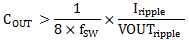
Equation 28 calculates the minimum output capacitance needed to meet the output voltage ripple specification. Where fSW is the switching frequency, VOUTripple is the maximum allowable output voltage ripple, and Iripple is the inductor ripple current. In this case, the maximum output voltage ripple is 20 mV and the inductor ripple current is 1.8 A. Under these conditions, Equation 28 yields 22.5 µF.
Additional capacitance de-ratings for aging, temperature and DC bias should be factored in, which increases this minimum value. Capacitors generally have limits to the amount of ripple current they can handle without failing or producing excess heat. An output capacitor that can support the inductor ripple current must be specified. Some capacitor data sheets specify the RMS (Root Mean Square) value of the maximum ripple current. Equation 25 can be used to calculate the RMS ripple current the output capacitor needs to support. For this application, Equation 25 yields 519 mA.
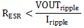
Equation 29 calculates the maximum ESR an output capacitor can have to meet the output voltage ripple specification. Equation 29 indicates the ESR should be less than 11.11 mΩ.
For this specific design, taking into consideration the stringent requirements for space applications, a total output capacitance of 2 mF with an equivalent ESR of approximately 2 mΩ has been selected.