SLVSFL2B May 2021 – December 2022 TPS7H4002-SP
PRODUCTION DATA
- 1 Features
- 2 Applications
- 3 Description
- 4 Revision History
- 5 Pin Configuration and Functions
- 6 Specifications
-
7 Detailed Description
- 7.1 Overview
- 7.2 Functional Block Diagram
- 7.3
Feature Description
- 7.3.1 VIN and Power VIN Pins (VIN and PVIN)
- 7.3.2 Voltage Reference
- 7.3.3 Adjusting the Output Voltage
- 7.3.4 Safe Start-Up Into Prebiased Outputs
- 7.3.5 Error Amplifier
- 7.3.6 Slope Compensation
- 7.3.7 Enable and Adjust UVLO
- 7.3.8 Adjustable Switching Frequency and Synchronization (SYNC)
- 7.3.9 Slow Start (SS/TR)
- 7.3.10 Power Good (PWRGD)
- 7.3.11 Sequencing (SS/TR)
- 7.3.12 Output Overvoltage Protection (OVP)
- 7.3.13 Overcurrent Protection
- 7.3.14 Thermal Shutdown
- 7.3.15 Turn-On Behavior
- 7.3.16 Small Signal Model for Frequency Compensation
- 7.4 Device Functional Modes
-
8 Application and Implementation
- 8.1 Application Information
- 8.2
Typical Application
- 8.2.1 Design Requirements
- 8.2.2
Detailed Design Procedure
- 8.2.2.1 Operating Frequency
- 8.2.2.2 Output Inductor Selection
- 8.2.2.3 Output Capacitor Selection
- 8.2.2.4 Output Schottky Diode
- 8.2.2.5 Slow Start Capacitor Selection
- 8.2.2.6 Undervoltage Lockout (UVLO) Set Point
- 8.2.2.7 Output Voltage Feedback Resistor Selection
- 8.2.2.8 Compensation Component Selection
- 8.2.3 Parallel Operation
- 8.2.4 Application Curve
- 9 Power Supply Recommendations
- 10Layout
- 11Device and Documentation Support
- 12Mechanical, Packaging, and Orderable Information
Package Options
Mechanical Data (Package|Pins)
- HKH|20
- KGD|0
Thermal pad, mechanical data (Package|Pins)
Orderable Information
8.2.2.3 Output Capacitor Selection
There are three primary considerations for selecting the value of the output capacitor. The output capacitor determines the modulator pole, the output voltage ripple, and how the regulator responds to a large change in load current. The output capacitance needs to be selected based on the more stringent of these three criteria.
The desired response to a large change in the load current is the first criteria. The output capacitor needs to supply the load with current when the regulator can not. This situation would occur if there are desired hold-up times for the regulator where the output capacitor must hold the output voltage above a certain level for a specified amount of time after the input power is removed. The regulator is also temporarily not able to supply sufficient output current if there is a large, fast increase in the current needs of the load such as a transition from no load to full load. The output capacitor must be sized to supply the extra current to the load until the control loop responds to the load change. Equation 14 shows the minimum output capacitance, from the electrical point of view, necessary to accomplish this.
Where ΔIO is the change in output current, fSW is the regulator switching frequency and ΔVOUT is the allowable change in the output voltage. For this example, the transient load response is specified as a 3% change in VOUT for a load step of 1.5 A. For this example, ΔIO = 1.5 A and ΔVOUT = 0.05 × 2.5 = 0.125 V. Using these numbers gives a minimum capacitance of 80 μF. This value does not take the ESR of the output capacitor into account in the output voltage change. For ceramic capacitors, the ESR is usually small enough to ignore in this calculation. However, for space applications and large capacitance values, tantalum capacitors are typically used which have a certain ESR value to take into consideration.
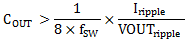
Equation 15 calculates the minimum output capacitance needed to meet the output voltage ripple specification. Where fSW is the switching frequency, VOUTripple is the maximum allowable output voltage ripple, and Iripple is the inductor ripple current. In this case, the maximum output voltage ripple is 20 mV. Under this requirement, Equation 15 yields 15 µF.
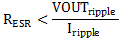
Equation 16 calculates the maximum ESR an output capacitor can have to meet the output voltage ripple specification. Equation 16 indicates the ESR should be less than 16.7 mΩ.
For this specific design, taking into consideration the stringent requirements for space applications, an output capacitor of 330 µF with ESR = 6 mΩ has been selected.