SLVSFL2B May 2021 – December 2022 TPS7H4002-SP
PRODUCTION DATA
- 1 Features
- 2 Applications
- 3 Description
- 4 Revision History
- 5 Pin Configuration and Functions
- 6 Specifications
-
7 Detailed Description
- 7.1 Overview
- 7.2 Functional Block Diagram
- 7.3
Feature Description
- 7.3.1 VIN and Power VIN Pins (VIN and PVIN)
- 7.3.2 Voltage Reference
- 7.3.3 Adjusting the Output Voltage
- 7.3.4 Safe Start-Up Into Prebiased Outputs
- 7.3.5 Error Amplifier
- 7.3.6 Slope Compensation
- 7.3.7 Enable and Adjust UVLO
- 7.3.8 Adjustable Switching Frequency and Synchronization (SYNC)
- 7.3.9 Slow Start (SS/TR)
- 7.3.10 Power Good (PWRGD)
- 7.3.11 Sequencing (SS/TR)
- 7.3.12 Output Overvoltage Protection (OVP)
- 7.3.13 Overcurrent Protection
- 7.3.14 Thermal Shutdown
- 7.3.15 Turn-On Behavior
- 7.3.16 Small Signal Model for Frequency Compensation
- 7.4 Device Functional Modes
-
8 Application and Implementation
- 8.1 Application Information
- 8.2
Typical Application
- 8.2.1 Design Requirements
- 8.2.2
Detailed Design Procedure
- 8.2.2.1 Operating Frequency
- 8.2.2.2 Output Inductor Selection
- 8.2.2.3 Output Capacitor Selection
- 8.2.2.4 Output Schottky Diode
- 8.2.2.5 Slow Start Capacitor Selection
- 8.2.2.6 Undervoltage Lockout (UVLO) Set Point
- 8.2.2.7 Output Voltage Feedback Resistor Selection
- 8.2.2.8 Compensation Component Selection
- 8.2.3 Parallel Operation
- 8.2.4 Application Curve
- 9 Power Supply Recommendations
- 10Layout
- 11Device and Documentation Support
- 12Mechanical, Packaging, and Orderable Information
Package Options
Mechanical Data (Package|Pins)
- HKH|20
- KGD|0
Thermal pad, mechanical data (Package|Pins)
Orderable Information
7.3.11 Sequencing (SS/TR)
Many of the common power-supply sequencing methods can be implemented using the SS/TR, EN, and PWRGD pins.
The sequential method is shown in Figure 7-5 using two TPS7H4002-SP devices. The power good of the first device is coupled to the EN pin of the second device, which enables the second power supply after the primary supply reaches regulation.
Figure 7-6 shows the method implementing ratiometric sequencing by connecting the SS/TR pins of two devices together. The regulator outputs ramp up and reach regulation at the same time. When calculating the slow-start time, the pullup current source must be doubled in Equation 5.
 Figure 7-6 Ratiometric Start-Up Sequence
Ratiometric and simultaneous power-supply sequencing can be implemented by connecting the resistor network of R1 and R2 (shown in Figure 7-7) to the output of the power supply that needs to be tracked or another voltage reference source. Using Equation 6 and Equation 7, the tracking resistors can be calculated to initiate the VOUT2 slightly before, after, or at the same time as VOUT1. Equation 8 is the voltage difference between VOUT1 and VOUT2.
To design a ratiometric start-up in which the VOUT2 voltage is slightly greater than the VOUT1 voltage when VOUT2 reaches regulation, use a negative number in Equation 6 and Equation 7 for ΔV. Equation 8 results in a positive number for applications where the VOUT2 is slightly lower than VOUT1 when VOUT2 regulation is achieved.
The ΔV variable is 0 V for simultaneous sequencing. To minimize the effect of the inherent SS/TR to VSENSE offset ( VSS-OFFSET, 30 mV) in the slow-start circuit and the offset created by the pullup current source (ISS = 2.5 μA) and tracking resistors, the VSS-OFFSET and ISS are included as variables in the equations.
To ensure proper operation of the device, the calculated R1 value from Equation 6 must be greater than the value calculated in Equation 9.
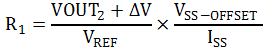
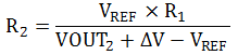
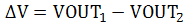

 Figure 7-7 Ratiometric and Simultaneous Start-Up Sequence