SLVSFL2B May 2021 – December 2022 TPS7H4002-SP
PRODUCTION DATA
- 1 Features
- 2 Applications
- 3 Description
- 4 Revision History
- 5 Pin Configuration and Functions
- 6 Specifications
-
7 Detailed Description
- 7.1 Overview
- 7.2 Functional Block Diagram
- 7.3
Feature Description
- 7.3.1 VIN and Power VIN Pins (VIN and PVIN)
- 7.3.2 Voltage Reference
- 7.3.3 Adjusting the Output Voltage
- 7.3.4 Safe Start-Up Into Prebiased Outputs
- 7.3.5 Error Amplifier
- 7.3.6 Slope Compensation
- 7.3.7 Enable and Adjust UVLO
- 7.3.8 Adjustable Switching Frequency and Synchronization (SYNC)
- 7.3.9 Slow Start (SS/TR)
- 7.3.10 Power Good (PWRGD)
- 7.3.11 Sequencing (SS/TR)
- 7.3.12 Output Overvoltage Protection (OVP)
- 7.3.13 Overcurrent Protection
- 7.3.14 Thermal Shutdown
- 7.3.15 Turn-On Behavior
- 7.3.16 Small Signal Model for Frequency Compensation
- 7.4 Device Functional Modes
-
8 Application and Implementation
- 8.1 Application Information
- 8.2
Typical Application
- 8.2.1 Design Requirements
- 8.2.2
Detailed Design Procedure
- 8.2.2.1 Operating Frequency
- 8.2.2.2 Output Inductor Selection
- 8.2.2.3 Output Capacitor Selection
- 8.2.2.4 Output Schottky Diode
- 8.2.2.5 Slow Start Capacitor Selection
- 8.2.2.6 Undervoltage Lockout (UVLO) Set Point
- 8.2.2.7 Output Voltage Feedback Resistor Selection
- 8.2.2.8 Compensation Component Selection
- 8.2.3 Parallel Operation
- 8.2.4 Application Curve
- 9 Power Supply Recommendations
- 10Layout
- 11Device and Documentation Support
- 12Mechanical, Packaging, and Orderable Information
Package Options
Mechanical Data (Package|Pins)
- HKH|20
- KGD|0
Thermal pad, mechanical data (Package|Pins)
Orderable Information
7.3.16 Small Signal Model for Frequency Compensation
The device uses a transconductance amplifier for the error amplifier and readily supports two of the commonly used frequency compensation circuits shown in Figure 7-8. In Type 2A, one additional high-frequency pole is added to attenuate high-frequency noise.
The following design guidelines are provided for advanced users who prefer to compensate using the general method. The step-by-step design procedure described in Detailed Design Procedure may also be used.
 Figure 7-8 Types of Frequency Compensation
The general design guidelines for device loop compensation are as follows:
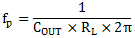
- Determine the crossover frequency fco. A good starting point is one-tenth of the switching frequency, ƒSW.
- R3 can be determined by:
Equation 10.

where gmea is the gm of the error amplifier (1400 μS), gmps is the gm of the power stage (12 S) and VREF is the reference voltage (0.807 V).
- Place a compensation zero at the dominant pole
 using C1 and R3.
C1 can be determined byEquation 11.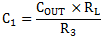
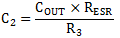
- C2 is optional. It can be used to cancel the zero from the equivalent series resistance (ESR) of the output capacitor COUT.
Equation 12.