SLVSFL2B May 2021 – December 2022 TPS7H4002-SP
PRODUCTION DATA
- 1 Features
- 2 Applications
- 3 Description
- 4 Revision History
- 5 Pin Configuration and Functions
- 6 Specifications
-
7 Detailed Description
- 7.1 Overview
- 7.2 Functional Block Diagram
- 7.3
Feature Description
- 7.3.1 VIN and Power VIN Pins (VIN and PVIN)
- 7.3.2 Voltage Reference
- 7.3.3 Adjusting the Output Voltage
- 7.3.4 Safe Start-Up Into Prebiased Outputs
- 7.3.5 Error Amplifier
- 7.3.6 Slope Compensation
- 7.3.7 Enable and Adjust UVLO
- 7.3.8 Adjustable Switching Frequency and Synchronization (SYNC)
- 7.3.9 Slow Start (SS/TR)
- 7.3.10 Power Good (PWRGD)
- 7.3.11 Sequencing (SS/TR)
- 7.3.12 Output Overvoltage Protection (OVP)
- 7.3.13 Overcurrent Protection
- 7.3.14 Thermal Shutdown
- 7.3.15 Turn-On Behavior
- 7.3.16 Small Signal Model for Frequency Compensation
- 7.4 Device Functional Modes
-
8 Application and Implementation
- 8.1 Application Information
- 8.2
Typical Application
- 8.2.1 Design Requirements
- 8.2.2
Detailed Design Procedure
- 8.2.2.1 Operating Frequency
- 8.2.2.2 Output Inductor Selection
- 8.2.2.3 Output Capacitor Selection
- 8.2.2.4 Output Schottky Diode
- 8.2.2.5 Slow Start Capacitor Selection
- 8.2.2.6 Undervoltage Lockout (UVLO) Set Point
- 8.2.2.7 Output Voltage Feedback Resistor Selection
- 8.2.2.8 Compensation Component Selection
- 8.2.3 Parallel Operation
- 8.2.4 Application Curve
- 9 Power Supply Recommendations
- 10Layout
- 11Device and Documentation Support
- 12Mechanical, Packaging, and Orderable Information
Package Options
Mechanical Data (Package|Pins)
- HKH|20
- KGD|0
Thermal pad, mechanical data (Package|Pins)
Orderable Information
8.2.2.2 Output Inductor Selection
To calculate the value of the output inductor, use Equation 13. KL is a coefficient that represents the amount of inductor ripple current relative to the maximum output current, IO. The inductor ripple current is filtered by the output capacitor therefore, choosing high inductor ripple currents impact the selection of the output capacitor since the output capacitor must have a ripple current rating equal to or greater than the inductor ripple current. In general, the inductor ripple value is at the discretion of the designer depending on specific system needs. Typical values for KL range from 0.1 to 0.5. For low output currents, the value of KL could be increased to reduce the value of the output inductor.
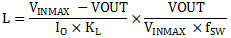
For this design example, use KL = 0.4 and the inductor value is calculated to be 2.2 µH for nominal VIN = 5 V.